
Semiconductor device

a technology of semiconductor devices and semiconductors, applied in semiconductor devices, semiconductor/solid-state device details, radiation control devices, etc., can solve the problems of increasing contact resistance, difficult to make direct contact between cu electrodes, and difficult to stably and continuously implement the set conditions, so as to achieve reliable bonding surface and enhance the bond strength between the first wiring layer and the second wiring layer

Active Publication Date: 2018-04-05
SONY CORP
View PDF32 Cites 5 Cited by
  • Summary
  • Abstract
  • Description
  • Claims
  • Application Information

AI Technical Summary

Benefits of technology

The present technology describes a semiconductor device that uses dummy electrodes to increase the area of metal bonding between two layers of wiring. This improves the strength of the bond and creates a more reliable surface for semiconductor device manufacturing.

Problems solved by technology

However, in an electrical connection between the semiconductor members, it is difficult to make direct contact between the Cu electrodes included in the respective semiconductor members and to secure flatness of bonding surfaces to such an extent that the bonding surfaces are allowed to be bonded together.
Moreover, it is difficult to stably and continuously implement the set conditions.
In this case, for example, a conduction failure or an increase in contact resistance may occur at the bonding interface Sj, and bondability may be considerably degraded accordingly.

Method used


Image

  • Semiconductor device
  • Semiconductor device
  • Semiconductor device

Examples


first embodiment

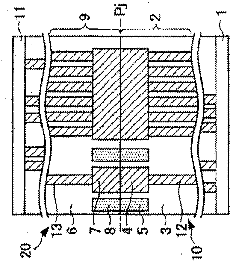
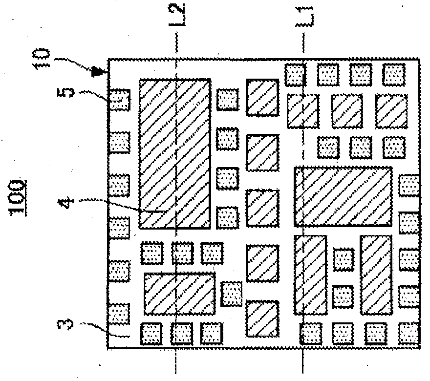
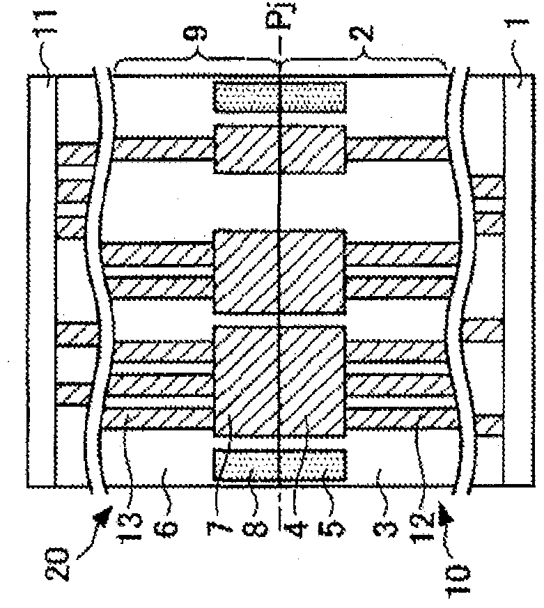
[0046]FIG. 1A is a schematic sectional view of a semiconductor device 100 according to a first embodiment. The semiconductor device 100 according to this embodiment includes a first semiconductor member 10 and a second semiconductor member 20 bonded to the first semiconductor member 10. Moreover, FIG. 1B is a diagram illustrating a bonding surface of the first semiconductor member 10, and FIG. 1A is a sectional view taken along a line L1 of FIG. 1B. Further, FIG. 1C is a sectional view taken along a line L2 of FIG. 1B.

[0047]As illustrated in FIGS. 1A and 1C, the first semiconductor member 10 includes, for example, a substrate 1 and a first wiring layer 2 formed on the substrate 1. Moreover, although not illustrated, for example, a semiconductor element such as a transistor or a diode is formed on the substrate 1. For example, a planarization film made of SiO2, NSG (nondoped silicate glass), PSG (phospho-silicate glass), or TEOS (tetraethoxysilane) is disposed on the semiconductor el...

second embodiment

[0059]In the first embodiment, the first electrode pads 4 and the second electrode pads 7, and the dummy electrode 5 and the dummy electrode 8 are disposed plane-symmetrically with respect to the bonding surface Pj. However, as described above, they are not necessarily disposed plane-symmetrically.

[0060]FIG. 2A is a diagram illustrating a bonding surface of the first semiconductor member 10 of a semiconductor device 200 according to a second embodiment and FIG. 2B is a diagram illustrating a bonding surface of the second semiconductor member 20. Moreover, FIG. 2C is a sectional view of the semiconductor device 200 taken along a line L3 illustrated in FIGS. 2A and 2B. It is to be noted that like components are denoted by like numerals as of the first embodiment, and will not be further described. Moreover, in this embodiment, configurations other than the first wiring layer 2 and the second wiring layer 9 are the same as those in the first embodiment (refer to FIG. 1C); therefore, in...

third embodiment

[0064]FIG. 3A is a diagram illustrating a bonding surface of the first semiconductor member 10 of a semiconductor device 300 according to a third embodiment, and FIG. 3B is a sectional view of the semiconductor device 300 taken along a line L4 illustrated in FIG. 3A. Moreover, in this embodiment, configurations other than the first wiring layer 2, the second wiring layer 9, a third wiring layer 18, and a fourth wiring layer 19 are the same as those in the first embodiment (refer to FIG. 1C); therefore, only these wiring layers are illustrated in FIG. 3B.

[0065]The semiconductor device 300 according to this embodiment includes the first semiconductor member 10 and the second semiconductor member 20. The first semiconductor member 10 includes the first wiring layer 2 and the third wiring layer 18. As illustrated in FIG. 3A, in this embodiment, the first electrode pads 4 and the dummy electrodes 5 in the first wiring layer 2 have the same bonding surface shape, and are all arranged at e...


PUM


Abstract

A first semiconductor device includes: a first wiring layer including a first interlayer insulating film, a first electrode pad, and a first dummy electrode, the first electrode pad being embedded in the first interlayer insulating film and having one surface located on same plane as one surface of the first interlayer insulating film, and the first dummy electrode being embedded in the first interlayer insulating film, having one surface located on same plane as the one surface of the first interlayer insulating film, and being disposed around the first electrode pad; and a second wiring layer including a second interlayer insulating film, a second electrode pad, and a second dummy electrode, the second electrode pad being embedded in the second interlayer insulating film, having one surface located on same surface as one surface of the second interlayer insulating film, and being bonded to the first electrode pad, and the second dummy electrode having one surface located on same plane as the surface located closer to the first interlayer insulating film of the second interlayer insulating film, being disposed around the second electrode pad, and being bonded to the first dummy electrode. A second semiconductor device includes: a first semiconductor section including a first electrode, the first electrode being formed on a surface located closer to a bonding interface and extending in a first direction; and a second semiconductor section including a second electrode and disposed to be bonded to the first semiconductor section at the bonding interface, the second electrode being bonded to the first electrode and extending in a second direction that intersects with the first direction.

Description

TECHNICAL FIELD[0001]The present technology relates to a semiconductor device in which two or more semiconductor members are bonded and laminated.BACKGROUND ART[0002]In related art, for example, in a case where a three-dimensional integrated circuit or the like is formed by bonding semiconductor members together, a method of directly bonding Cu electrodes disposed on bonding surfaces of the semiconductor members may be used (for example, refer to PTL 1, PTL 4, and PTL 5). For example, the following PTL 1 discloses bonding, through Cu electrodes (bonding pads), a first substrate in which a light reception element is formed and a second substrate in which a peripheral circuit is formed. In such a method, the Cu electrodes and interlayer insulating films that are included in the respective semiconductor members are planarized on a same plane and are bonded together, thereby bonding the facing Cu electrodes and the facing interlayer insulating films together.[0003]However, in an electri...

Claims


Application Information

Patent Timeline
Patent Type & Authority Applications(United States)
IPC IPC(8): H01L23/498H01L23/522H01L23/00H01L27/146H01L25/065H01L25/00
CPCH01L2924/12043H01L2924/00012H01L2924/13091H01L23/49866H01L23/498H01L2924/01029H01L2224/08123H01L2225/06565H01L2225/06513H01L2224/80896H01L2224/80895H01L2224/0616H01L2224/06133H01L2224/06131H01L2224/0603H01L25/50H01L25/0657H01L24/80H01L24/08H01L24/06H01L24/05H01L2224/08147H01L2224/80357H01L2224/06517H01L27/1464H01L27/14636H01L23/522H01L2224/05571H01L2224/05547H01L21/7684H01L2924/00014H01L2224/05552H01L2924/00H01L2224/80194H01L24/09H01L23/53238H01L2224/09517H01L27/14634H01L2224/08121H01L2224/0807H01L2224/08145H01L2224/08052H01L2224/80099H01L23/5226H01L23/5286H01L23/5283
Inventor FUJII, NOBUTOSHIKAGAWA, YOSHIHISA
Owner SONY CORP
Learn More