
Photosensitive Assembly and Camera Module and Manufacturing Method Thereof

a technology of camera modules and components, applied in the field of camera modules, can solve the problems of black spot formation, easy contamination of resistor-capacitor components, unnecessary space occupation, etc., and achieve the effect of flat mounting condition, reducing the back focal length of the packaged camera modul

Active Publication Date: 2018-01-04
NINGBO SUNNY OPOTECH CO LTD
View PDF1 Cites 23 Cited by
  • Summary
  • Abstract
  • Description
  • Claims
  • Application Information

AI Technical Summary

Benefits of technology

This invention provides a packaged camera module and its photosensitive assembly and manufacturing method. The photosensitive element and window circuit board are integrally packaged and overlapping, reducing the height of the module. The window circuit board has a window for the photosensitive element, minimizing the thickness. The bottom of the photosensitive element is exposed to improve heat dissipation. The photosensitive assembly includes an optical filter to shelter and protect the photosensitive element. The packaging body includes a lens portion extending upwardly and integrally, providing a flat and stable mounting condition. In some embodiments, the photosensitive element and window circuit board provide a gap, and the packaging body is integrally connected and filled between the gap to strengthen the connection.

Problems solved by technology

Firstly, in such a conventional manner, the photosensitive chip is attached on an upper surface of the circuit board.
Thirdly, the photosensitive chip is electrically connected to the circuit board through one or more gold wires and the resistor-capacitor components are protruded from the circuit board.
This results in unnecessary space occupation.
On the other hand, the resistor-capacitor components are easily contaminated with dust and debris, which does influence the imaging quality of the camera module and cause the formation of black spots.
However, in the above assembling process, the photosensitive chip, the circuit board and the resistor-capacitor components all take up space, which makes the size of the conventional camera module being very difficult to be reduced.

Method used


Image

  • Photosensitive Assembly and Camera Module and Manufacturing Method Thereof
  • Photosensitive Assembly and Camera Module and Manufacturing Method Thereof
  • Photosensitive Assembly and Camera Module and Manufacturing Method Thereof

Examples


first embodiment

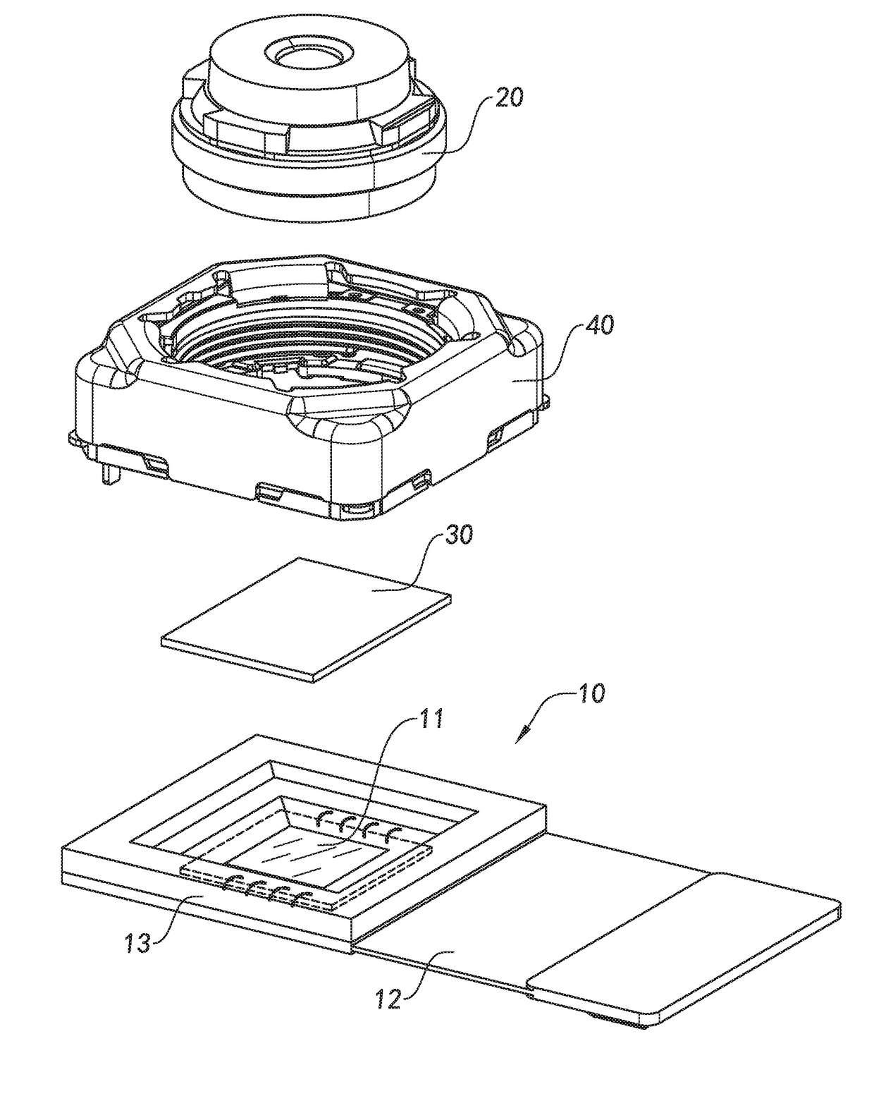
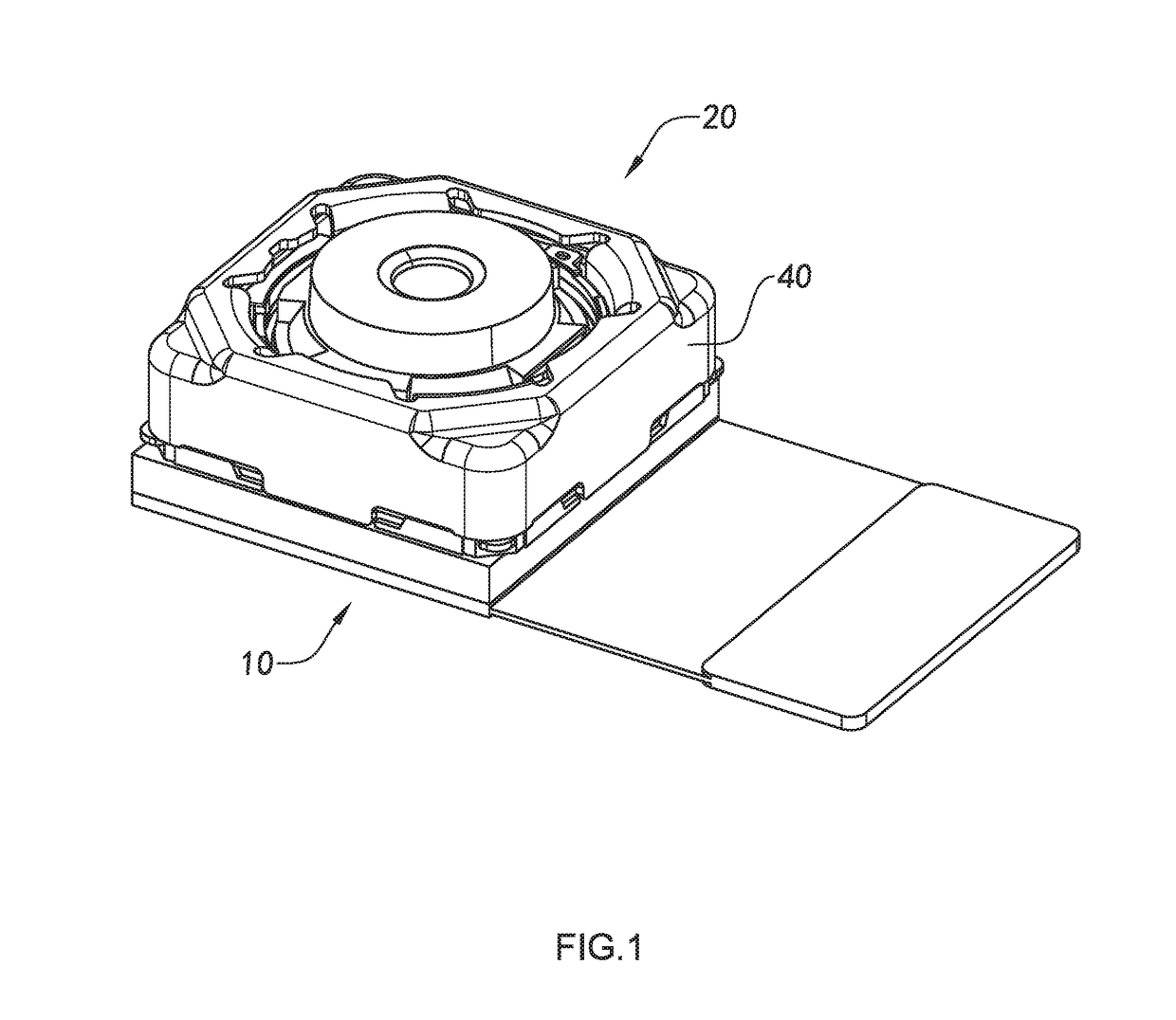
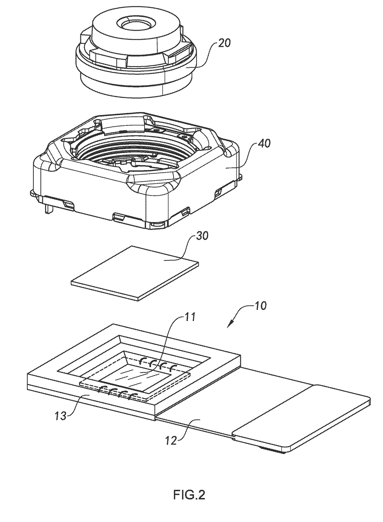
[0083]Further, the camera module may further include at least one driver 40, wherein driver 40 is mounted on the photosensitive assembly 10 while the lens 20 is installed within the driver 40 so as to position the lens 20 at the light sensing path of the photosensitive assembly 10 so that the focal length of the camera module can be adjusted by the driver 40. The driver 40 may be implemented as a motor, such as, but not limited to, a voice coil motor, a piezoelectric motor, and the like. In other words, in this first embodiment of the present invention, the camera module is an Automatic Focus Model (AFM). Of course, in other embodiments of the present invention, the camera module may also be other types, such as a Fix Focus Model (FFM). It should be understood by those skilled in the art that the camera module of the present invention should not be limited to the above-mentioned types.

[0084]The optical filter 30 may be an infrared cut filter, a wafer level infrared cutoff filter, or...

second embodiment

[0120]In this second embodiment of the present invention, the one or more electrical connectors 14 are electrically connected to the photosensitive element 11 and the board body 121. That is, the one or more electrical connectors 14 are connected with the top surface of the photosensitive element 11 disposed within the window 122A and the top surface of the circuit board 12 outside the window 122A.

[0121]As shown in FIG. 10, an alternative mode of photosensitive assembly 10 of the above second embodiment of the present invention is illustrated. The difference between this alternative mode and the above second embodiment is that the one or more electrical connectors 14 are disposed in the window 122A of the window circuit board 12 to connect the photosensitive element 11 with the window circuit board 12. Further, one end of each of the electrical connectors 14 is connected to the non-photosensitive area 1112 of the photosensitive element 11 and another end of the respective electrical...

third embodiment

[0123]As shown in FIGS. 11 and 12, a camera module according to a third preferred embodiment of the present invention is illustrated. The difference between this third embodiment and the above embodiments is that the photosensitive assembly 10 includes an optical filter 30B which is directly provided on the photosensitive element 11. That is, the optical filter 30B covers and shields the photosensitive element 11, so as to further reduce any possible contamination of the photosensitive element 11 and damage to the photosensitive element 11 resulting from the mould during the molding and packaging process.

[0124]In this third embodiment, the top surface of the packaging body 13 may be a flat and planar surface without the step structure for installing the optical filter as embodied in the above first and second embodiments, wherein the lens or the driver 40 is mounted on the packaging body 13.

[0125]For example, the optical filter 30B may be attached to the photosensitive element 11 by...


PUM


Abstract

A camera module and its photosensitive assembly and manufacturing method thereof are provided. The photosensitive assembly includes a photosensitive element, a window circuit board and a packaging body integrally packaged the photosensitive element and the window circuit board to form an integrated body, wherein the window circuit board has at least one window for receiving the photosensitive element therein.

Description

CROSS REFERENCE OF RELATED APPLICATION[0001]This is a non-provisional application that claims priority under 35 U.S.C. 119(a-d) to Chinese application number CN 201610516600.2, filed Jul. 3, 2016 and Chinese application number CN 201620691699.5, filed Jul. 3, 2016, the entire contents of each of which are expressly incorporated herein by reference.NOTICE OF COPYRIGHT[0002]A portion of the disclosure of this patent document contains material which is subject to copyright protection. The copyright owner has no objection to any reproduction by anyone of the patent disclosure, as it appears in the United States Patent and Trademark Office patent files or records, but otherwise reserves all copyright rights whatsoever.BACKGROUND OF THE PRESENT INVENTIONField of Invention[0003]The present invention relates to camera module, and more particularly to a molded camera module and its photosensitive assembly and manufacturing method thereof.Description of Related Arts[0004]The conventional came...

Claims


Application Information

Patent Timeline
Patent Type & Authority Applications(United States)
IPC IPC(8): H04N5/225
CPCH04N5/2252H04N5/2257H04N5/2254H04N23/51H04N23/57H04N23/55H04N23/54
Inventor WANG, MINGZHUCHEN, ZHENYUTANAKA, TAKEHIKOLUAN, ZHONGYUZHAO, BOJIEHUANG, ZHENGUO, NANXI, FENGSHENGJIANG, HENGDENG, ZILONG
Owner NINGBO SUNNY OPOTECH CO LTD
Learn More