Milimeter-wave transmission device
- Summary
- Abstract
- Description
- Claims
- Application Information
AI Technical Summary
Benefits of technology
Problems solved by technology
Method used
Image
Examples
Embodiment Construction
[0031]The same elements have been designated with the same reference numerals in the various drawings and, further, the various drawings are not to scale. For clarity, only those steps and elements which are useful to the understanding of the described embodiments have been shown and are detailed.
[0032]Unless otherwise specified, expression “in the order of” means to within 10%, preferably to within 5%.
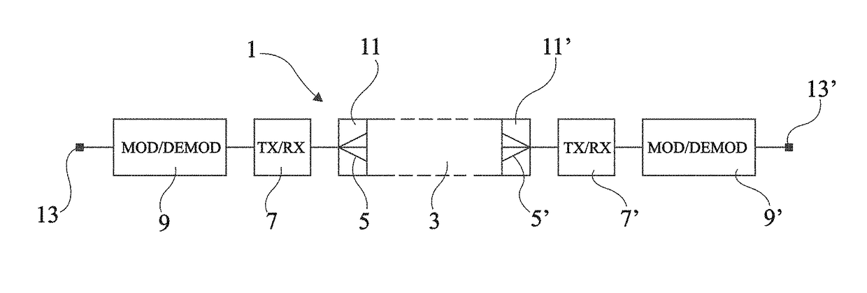
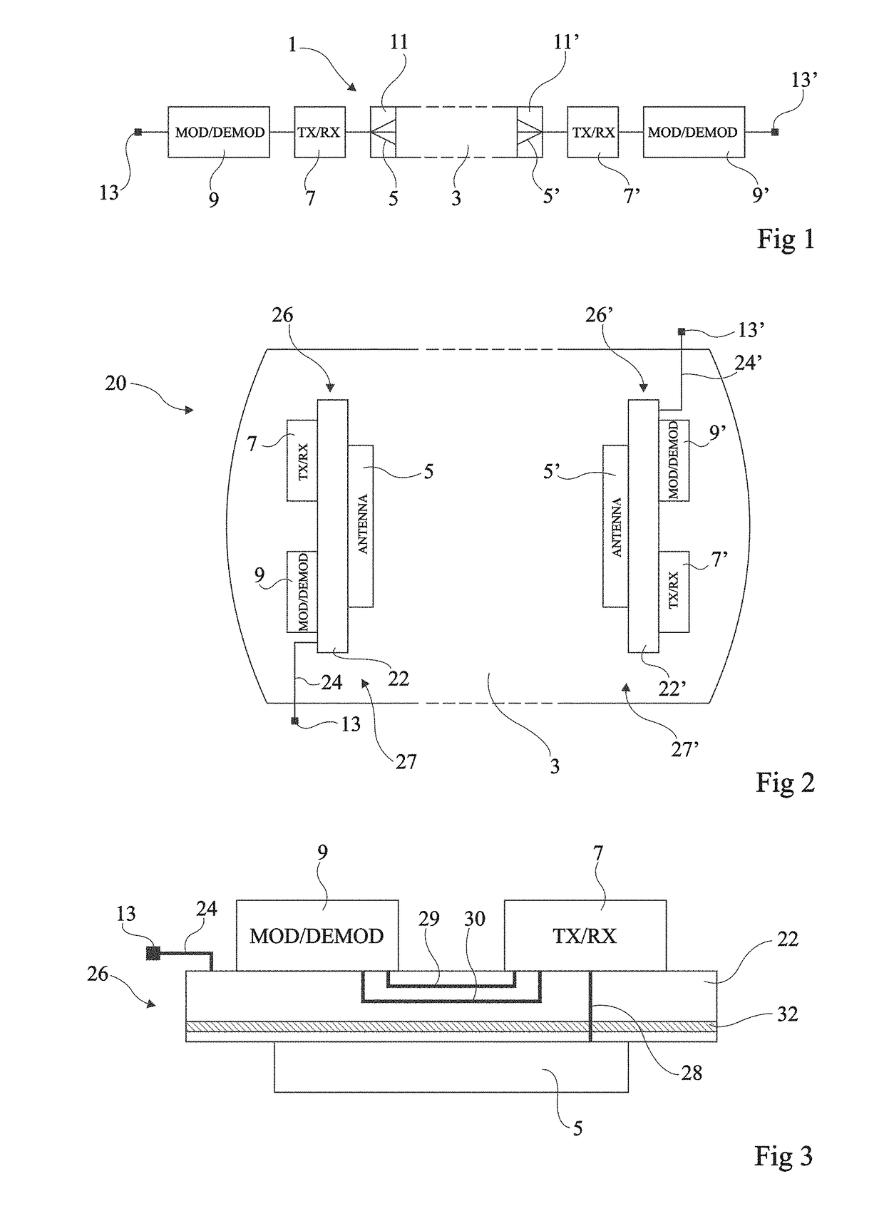
[0033]FIG. 2 is a diagram illustrating an embodiment of a millimeter-wave transmission device 20. Device 20 comprises the same elements as the millimeter-wave transmission system described in FIG. 1, that is, a waveguide 3 made of a dielectric plastic material, antennas 5 and 5′, transceiver circuits (TX / RX) 7 and 7′, modulation-demodulation circuits (MOD / DEMOD) 9 and 9′, and input-output terminals 13 and 13′.
[0034]The dielectric constant of the material of waveguide 3 is for example in the range from 1 to 4, preferably in the range from 2 to 4. The loss angle or delta tangent of the ...
PUM
 Abstract
Description
Claims
Application Information
 - R&D
- Intellectual Property
- Life Sciences
- Materials
- Tech Scout
- Unparalleled Data Quality
- Higher Quality Content
- 60% Fewer Hallucinations
Browse by: Latest US Patents, China's latest patents, Technical Efficacy Thesaurus, Application Domain, Technology Topic, Popular Technical Reports.
© 2025 PatSnap. All rights reserved.Legal|Privacy policy|Modern Slavery Act Transparency Statement|Sitemap|About US| Contact US: help@patsnap.com


