
Optical modulator

a technology of optical modulator and optical axis, applied in non-linear optics, instruments, optics, etc., can solve problems such as increased substrate size, and achieve the effect of high capacity required for communication

Active Publication Date: 2017-09-28
SUMITOMO OSAKA CEMENT CO LTD
View PDF0 Cites 0 Cited by
  • Summary
  • Abstract
  • Description
  • Claims
  • Application Information

AI Technical Summary

Benefits of technology

The patent text describes an optical modulator that has multiple optical modulation sections in one substrate. Each section has its own modulation electrode to apply a different modulation signal. A multi-element structure optical modulator has also been developed, which includes multiple substrates each with a plurality of optical modulation sections. The optical modulator includes multiple light-receiving elements for monitoring each section and independently controlling the modulation signal. The text also proposes the formation of various structures between the waveguides to prevent optical crosstalk. The technical effects of this patent include higher capacity, improved signal quality, and more efficient and flexible optical communication systems.

Problems solved by technology

However, when disposing a plurality of light-receiving elements in the substrate, an increase in the substrate size is caused, and this increase becomes problematic in progress of the reduction in size of the substrate.

Method used


Image

  • Optical modulator
  • Optical modulator
  • Optical modulator

Examples


Embodiment Construction

[0031]Hereinafter, an optical modulator according to the invention will be described in detail.

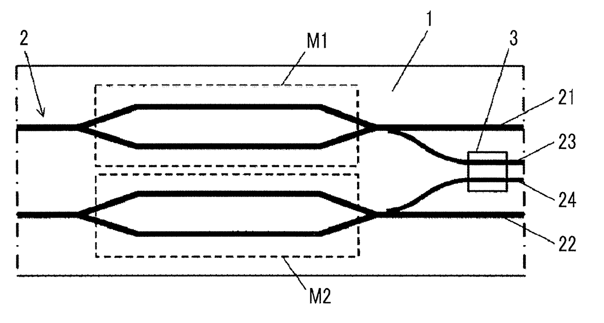
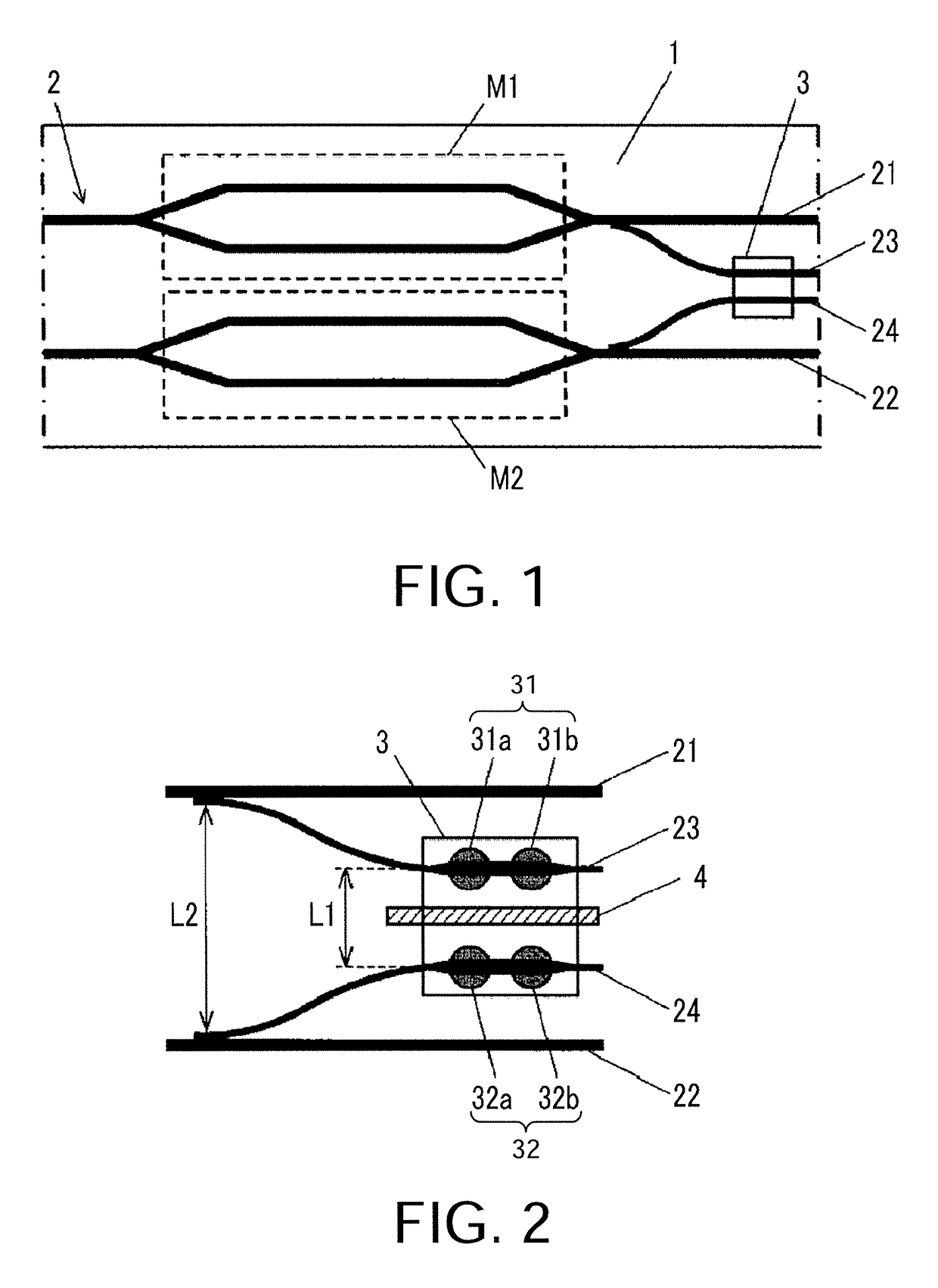
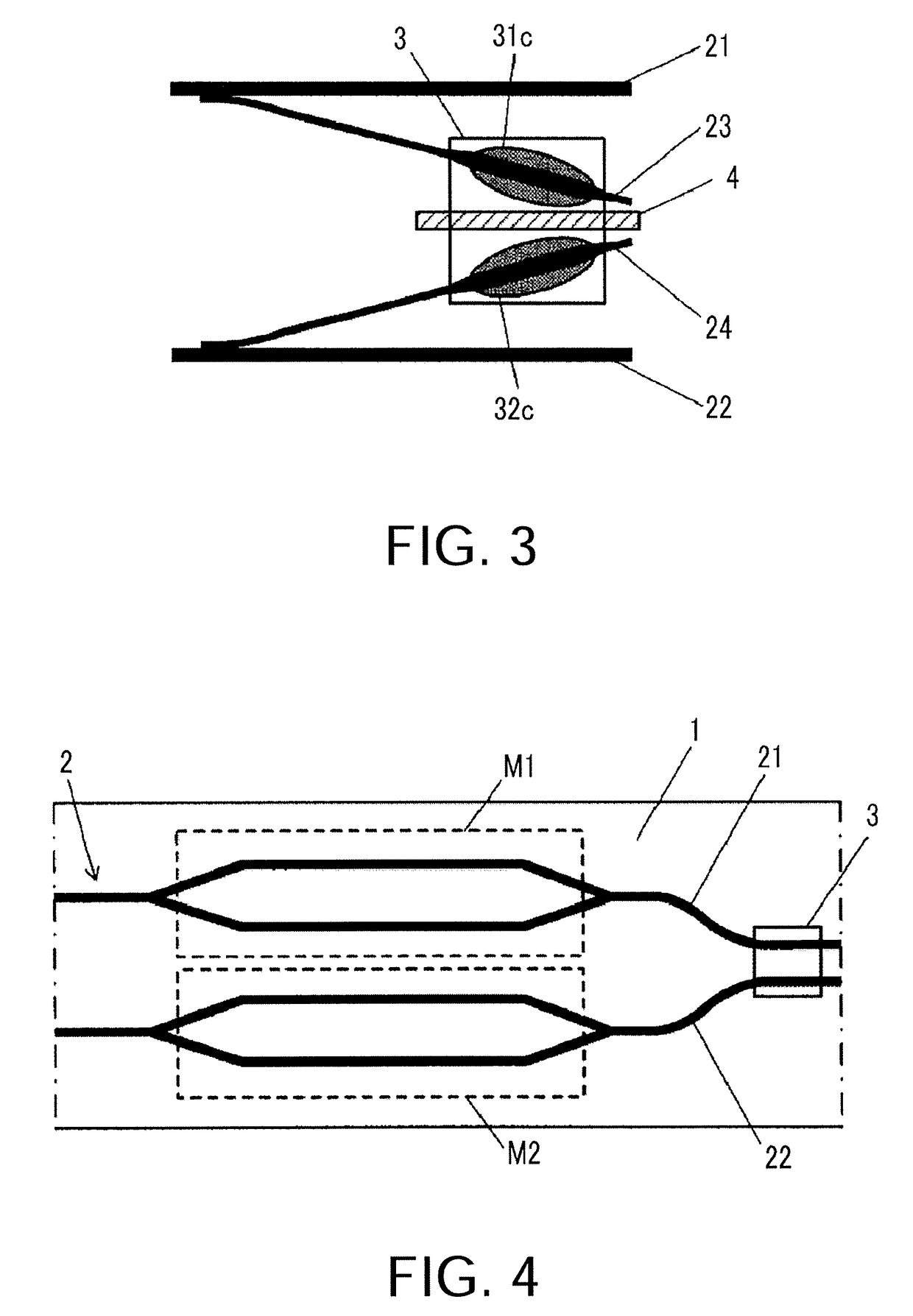
[0032]FIG. 1 is a plan view illustrating an optical modulator according to an example of the invention. FIG. 2 is an enlarged plan view of a light-receiving element portion in FIG. 1.

[0033]As illustrated in FIG. 1 and FIG. 2, the optical modulator of the invention relates to an optical modulator including a substrate 1 having an electro-optic effect, an optical waveguide 2 that is formed in the substrate, and a modulation electrode (not illustrated) for modulating a light wave that propagates through the optical waveguide.

[0034]The optical modulator includes at least a first optical modulation section M1 and a second optical modulation section M2 which use modulation signals different from each other when applying a modulation signal to the modulation electrode and performing optical modulation. In addition, a light-receiving element 3 is provided in the substrate, and the light-receiving ...


PUM

PropertyMeasurementUnit
refractive indexaaaaaaaaaa
thicknessaaaaaaaaaa
opticalaaaaaaaaaa

Abstract

An optical modulator includes a first optical modulation section and a second optical modulation section which use modulation signals different from each other when applying a modulation signal to the modulation electrode and performing optical modulation. In addition, a light-receiving element is disposed on a substrate, and the light-receiving element has a first light-receiving section that detects optical signal propagating from a first waveguide which guides the optical signal output from the first optical modulation section. In addition, the light-receiving element also has a second light-receiving section that detects an optical signal propagating through a second waveguide which guides the optical signal output from the second optical modulation section.

Description

CROSS-REFERENCE TO RELATED APPLICATION[0001]This application claims the priority benefit of Japan application serial no. 2016-061199, filed on Mar. 25, 2016. The entirety of the above-mentioned patent application is hereby incorporated by reference herein and made a part of this specification.BACKGROUND OF THE INVENTION[0002]Field of the Invention[0003]The present invention relates to an optical modulator, and particularly, to an optical modulator including a substrate having an electro-optic effect, an optical waveguide that is formed in the substrate, and a modulation electrode for modulating a light wave that propagates through the optical waveguide.[0004]Description of Related Art[0005]In an optical communication field or an optical measurement field, various kinds of optical modulator such as an intensity modulator and a phase modulator, which includes a Mach-Zehnder type optical waveguide, have been used. An intensity variation of light, which is output from the Mach-Zehnder t...

Claims


Application Information

Patent Timeline
Patent Type & Authority Applications(United States)
IPC IPC(8): G02F1/03G02F1/225
CPCG02F1/0327G02F1/225G02F2001/212G02F2201/58G02F1/0316G02F1/035G02F1/21G02F1/212G02F2201/18
Inventor KATOU, KEIMIYAZAKI, NORIKAZUSHIMIZU, RYO
Owner SUMITOMO OSAKA CEMENT CO LTD
Learn More