Semiconductor device and manufacturing method for the same

Active Publication Date: 2017-09-07
SK HYNIX INC
View PDF2 Cites 5 Cited by
  • Summary
  • Abstract
  • Description
  • Claims
  • Application Information

AI Technical Summary

Benefits of technology

The patent is about a semiconductor device and a way to make it more reliable. This will be helpful for people who need to use this device in their own products.

Problems solved by technology

A substrate may be damaged by an over etch in an area in which the slits overlap with each other, or a bottom of the slit may be too close to the substrate.

Method used


Image

  • Semiconductor device and manufacturing method for the same
  • Semiconductor device and manufacturing method for the same
  • Semiconductor device and manufacturing method for the same

Examples


Embodiment Construction

[0020]Embodiments are provided to transfer the spirit and the scope of the disclosure to those skilled in the art to which the disclosure pertains. Accordingly, it will be understood by those of skill in the art that various changes in form and details may be made without departing from the spirit and scope of the disclosure as set forth in the following claims. Therefore, the technical range of the present disclosure is not limited to the detailed description of the specification but defined by the range of the claims.

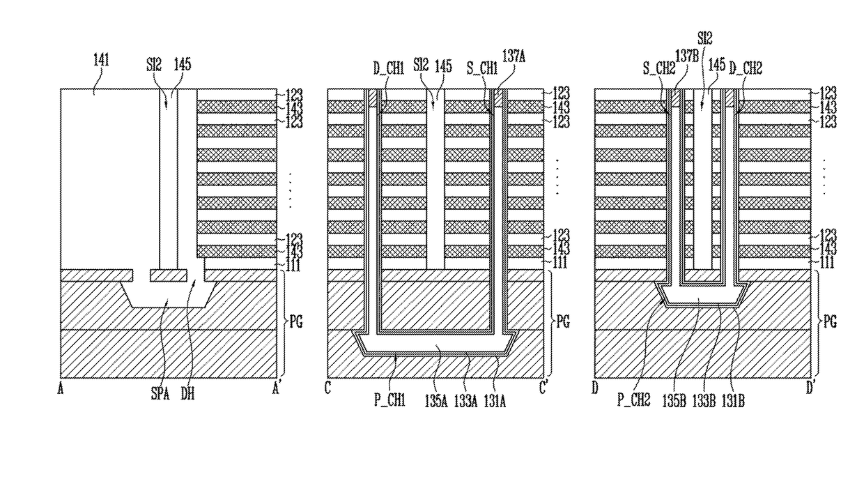
[0021]The present disclosure provides a semiconductor device improving an operational reliability thereof, and a method for manufacturing the same.

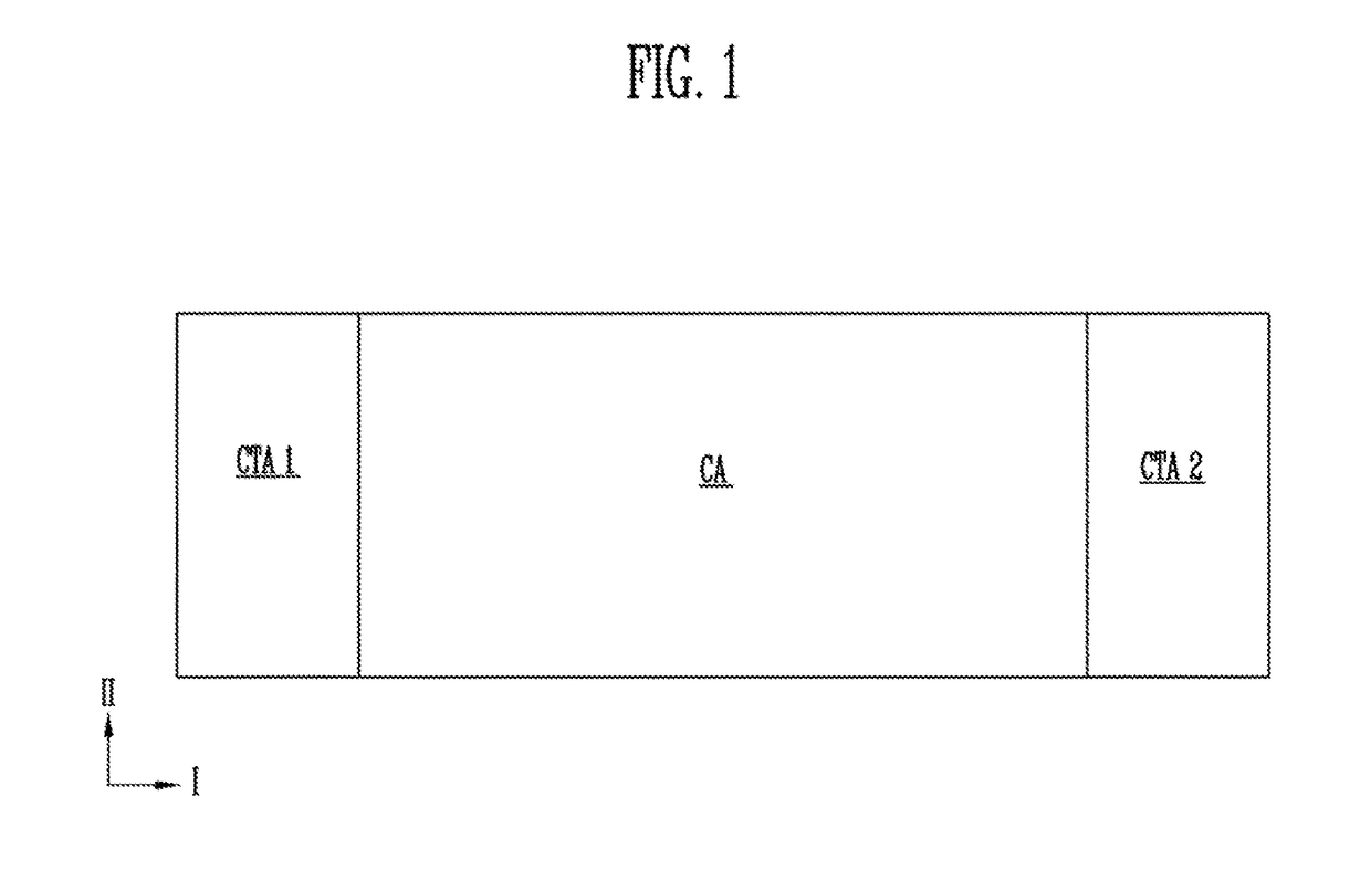
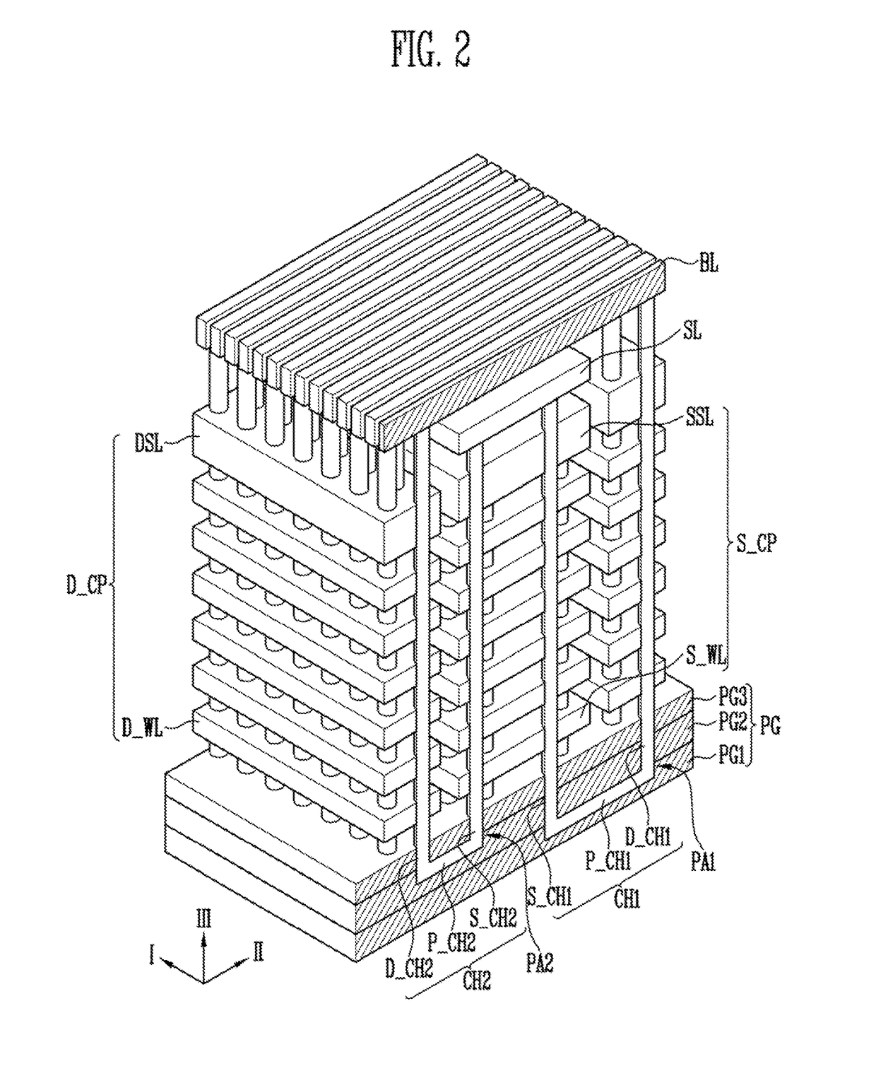
[0022]FIG. 1 illustrates a view of a cell area and a contact area of a memory device according to an embodiment of the present disclosure.

[0023]Referring to FIG. 1, the memory device according to the embodiment of the present disclosure may be formed over a substrate, the substrate including a cell area CA and contact areas...


PUM


Abstract

A semiconductor device includes interlayer insulating layers and conductive patterns alternately stacked over a pipe gate, a first slit and a second slit penetrating the interlayer insulating layers and the conductive patterns and crossing each other, an etch stop pad groove overlapping an intersection of the first slit and the second slit, arranged in the pipe gate, and connected to the first slit or the second slit, and slit insulating layers filling the first slit, the second slit and the etch stop pad groove.

Description

CROSS REFERENCE TO RELATED APPLICATION[0001]The present application claims a priority to a Korean patent application number 10-2016-0026537 filed on Mar. 4, 2016, the entire disclosure of which is incorporated herein by reference in its entirety.BACKGROUND1. Technical Field[0002]Embodiments of the present disclosure generally relate to a semiconductor device and a manufacturing method thereof, more particularly, to a three dimensional memory device and a method for manufacturing the same.[0003]2. Discussion of Related Arts[0004]The semiconductor device may include a memory device that stores data. The memory device may include memory cells. For a high integration of the semiconductor device, the memory cells may be arranged in three dimensions. The memory cells arranged in three dimensions may be coupled to conductive patterns arranged at different heights from each other. The conductive patterns may be penetrated by slits formed in a variety of shapes.[0005]The slits described abov...

Claims


Application Information

Patent Timeline
IPC IPC(8): H01L27/115H01L21/28H01L21/311
CPCH01L27/11578H01L27/11565H01L27/11582H01L21/28282H01L21/31144H10B41/10H10B41/00H10B43/35H10B43/27H01L29/40117H10B41/20H10B43/10H10B43/20H10B53/20
Inventor YOON, MYEONG SEONGSEO, IL SEOK
Owner SK HYNIX INC
Why Eureka
Try Eureka