Eureka AIR delivers breakthrough ideas for toughest innovation challenges, trusted by R&D personnel around the world.

Flexible organic light emitting diode display having edge bending structure

a light-emitting diode display and flexible technology, applied in the direction of photovoltaic energy generation, electrical equipment, semiconductor devices, etc., can solve the problems of overlapping portion deformation, reduce bending stress or weaken, prevent damage due to stack difference structure, and simplify manufacturing process

Active Publication Date: 2017-07-06
LG DISPLAY CO LTD
View PDF6 Cites 28 Cited by
  • Summary
  • Abstract
  • Description
  • Claims
  • Application Information

AI Technical Summary

Benefits of technology

This patent text describes a flexible display that can be bent without damaging the display elements. The non-display area can be moved behind the lateral side of the display by bending the boundary between the display area and non-display area. The display elements are not damaged by bending stress, and the manufacturing process is simplified by using a single etching process to form the trenches. The technical effects of this patent text are that the flexible display maintains its display function and is more durable and cost-effective to manufacture.

Problems solved by technology

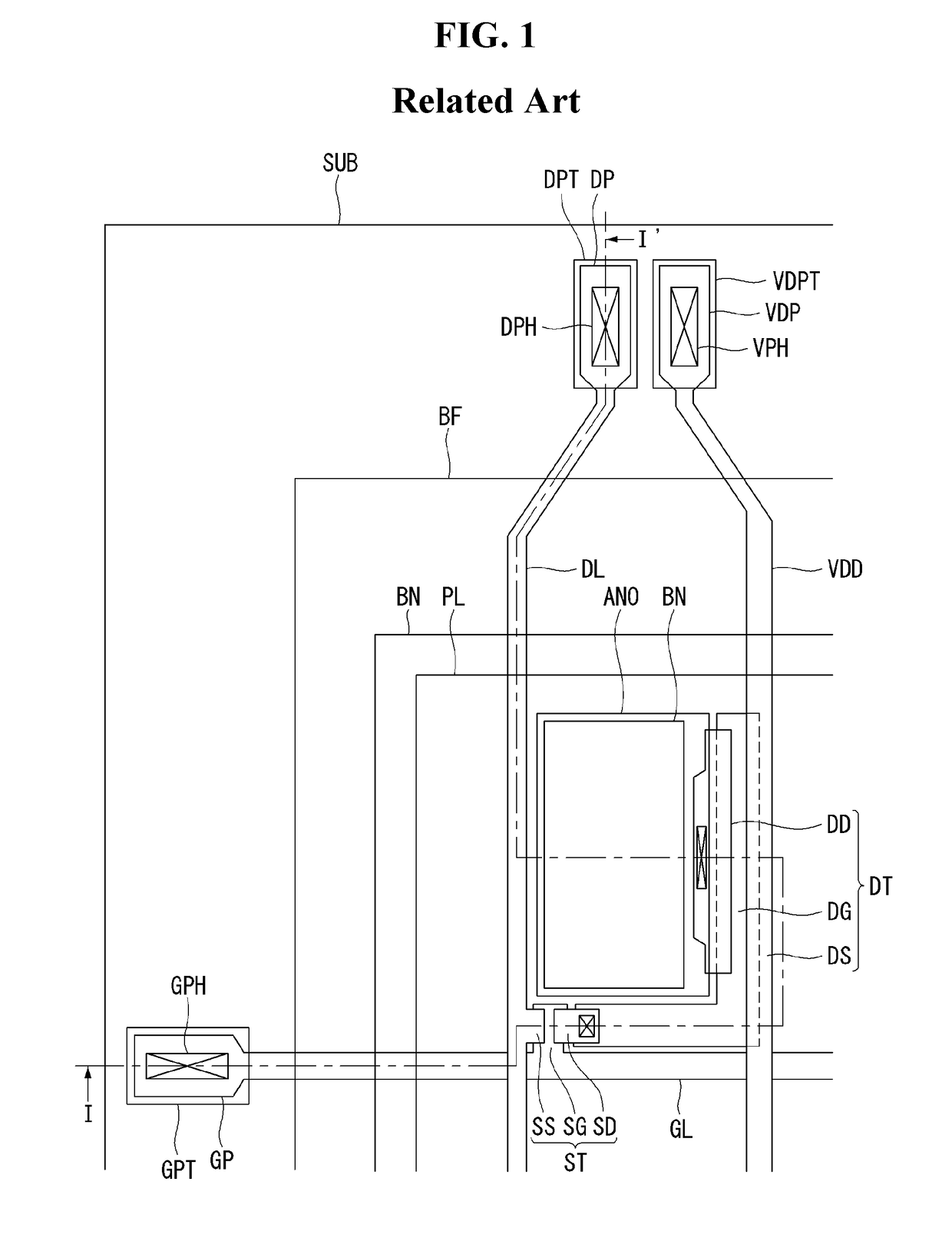
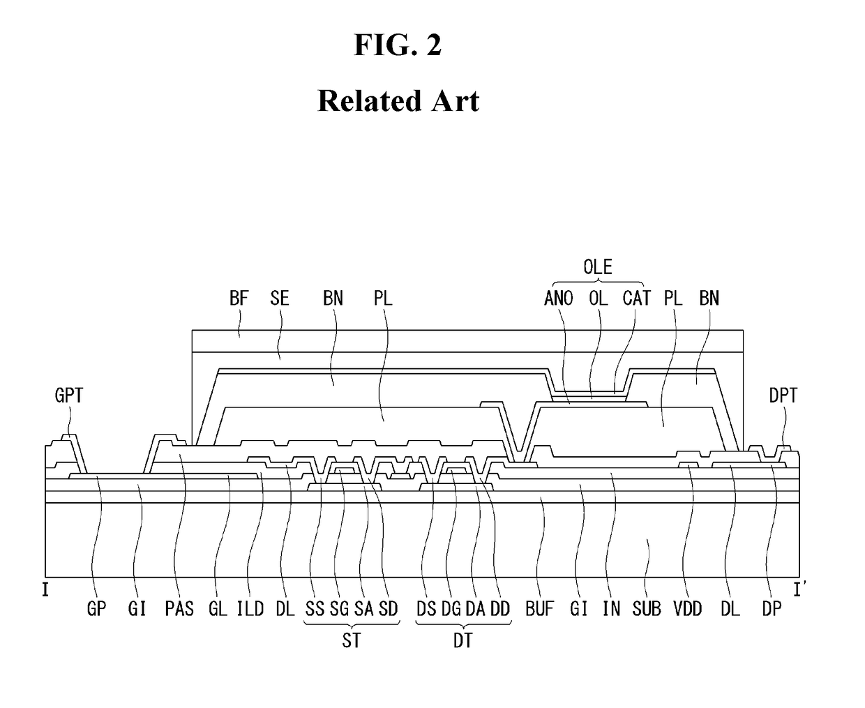
As the gate pad GP is disposed at the different layer from the data pad DP, some defects may occur at the overlapping portion due to the level difference.

Method used


Image

  • Flexible organic light emitting diode display having edge bending structure
  • Flexible organic light emitting diode display having edge bending structure
  • Flexible organic light emitting diode display having edge bending structure

Examples


first embodiment

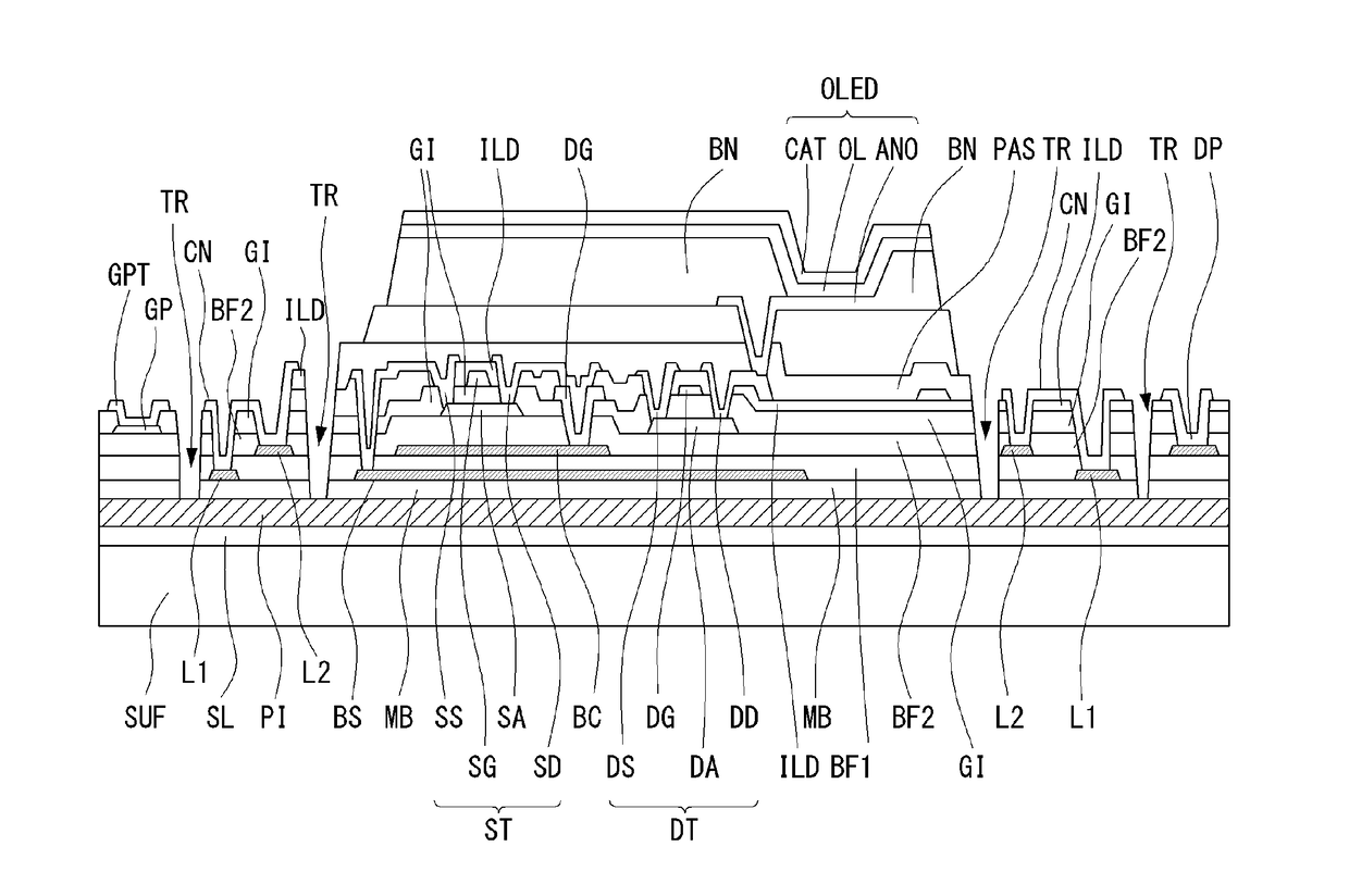
[0036]Referring to FIGS. 3, 4A and 4B, the first embodiment of the present disclosure will be explained. FIG. 3 is a plane view illustrating a structure of a flexible organic light emitting diode display having an edge bending structure according to the present disclosure. FIGS. 4A and 4B are cross sectional views illustrating the structure of a flexible organic light emitting diode display having an edge bending structure along the cutting line of II-IF in FIG. 3, according to the first embodiment of the present disclosure.

[0037]The flexible organic light emitting diode display according to the first embodiment of the present disclosure comprises a thin film transistor substrate on which thin film transistors ST and DT and an organic light emitting diode OLE driven by the thin film transistors ST and DT are formed. Further, a barrier plate attached on the thin film transistor substrate by a sealant may be included. The sealant and the barrier plate are not duplicately explained bec...

second embodiment

[0056]Hereinafter, referring to FIGS. 3, 5A and 5B the second embodiment will be explained. The second embodiment suggests a structure of the flexible organic light emitting diode display in which the defects which may be possibly associated with the first embodiment can be overcome or addressed. Some of the main features of the second embodiment are easily shown in the cross sectional view. Therefore, the structure in the plane view which is the same with the first embodiment will not be duplicated, and FIG. 3 is commonly used for the plane view. FIGS. 5A and 5B are cross sectional views illustrating a structure of a flexible organic light emitting diode display having an edge bending structure along the cutting line of II-IF in FIG. 3, according to the second embodiment of the present disclosure.

[0057]For the flexible organic light emitting diode display according to the second embodiment of the present disclosure, at first, the display elements are formed on a rigid substrate SUB...


PUM


Abstract

The present disclosure relates to a flexible organic light emitting diode display having an edge bending structure. The organic light emitting diode display according to an embodiment includes a flexible plate including a display area, a non-display area surrounding the display area, and an edge bending area near the display area in the non-display area; a first line disposed in the non-display area on the flexible plate; a first buffer layer covering the first line; a second line on the first buffer layer in the non-display area; a second buffer layer covering the second line; gate elements disposed on the second buffer layer; an intermediate insulating layer covering the gate elements; data elements, and a connecting electrode connecting the first line to the second line on the intermediate insulating layer; and a plurality of trenches disposed at the edge bending area and penetrating the intermediate insulating layer, the second buffer layer and the first buffer layer.

Description

CROSS REFERENCE TO RELATED APPLICATIONS[0001]This application claims the benefit of Korea Patent Application No. 10-2015-0189675 filed on Dec. 30, 2015, which is incorporated herein by reference for all purposes as if fully set forth herein.BACKGROUND OF THE INVENTION[0002]Field of the Invention[0003]The present disclosure relates to a flexible flat panel display. Especially, the present disclosure relates to a flexible organic light emitting diode display having edge bending structure.[0004]Discussion of the Related Art[0005]Nowadays, various flat panel display devices are developed for overcoming many drawbacks of the cathode ray tube such as heavy weight and bulk volume. The flat panel display devices include the liquid crystal display device (or LCD), the field emission display (or FED), the plasma display panel (or PDP) and the electroluminescence device (or EL).[0006]FIG. 1 is a plane view illustrating the structure of the organic light emitting diode display having the active...

Claims


Application Information

Patent Timeline
IPC IPC(8): H01L27/32H01L51/00
CPCH01L27/3258H01L51/0097H01L27/3262H01L27/3272H01L27/3276H10K59/12H10K77/111Y02E10/549H10K59/124H10K59/126H10K59/131H10K2102/311H10K59/1213
Inventor PARK, JAESOOSHIN, DONGCHAE
Owner LG DISPLAY CO LTD
Why Eureka
Eureka Blog
Learn More