
Organic electroluminescent device, manufacturing method thereof and electronic equipment

Active Publication Date: 2017-06-22
BOE TECH GRP CO LTD +1
View PDF13 Cites 4 Cited by
  • Summary
  • Abstract
  • Description
  • Claims
  • Application Information

AI Technical Summary

Benefits of technology

The present invention provides an organic electroluminescent device and a method of manufacturing it using a same substrate material for two light emitting layers. This results in a balanced injection of electrons and holes, leading to improved efficiency and lifetime of the device. The physical properties of the two layers are also matched, further enhancing the device's performance.

Problems solved by technology

However, there are some problems in the structure of top-emitting organic electroluminescent devices, such as low efficiency, high driving voltage, poor lifetime, viewing angle and so on.
However, it is difficult to obtain a light emitting material, of which the electron mobility and hole mobility are the same.
Due to the inconsistency between the electron-transport ability and hole-transport ability in the light emitting layer, the electrons and holes transported to the interface of the light emitting layer can not enter the light emitting layer and recombine with a same number, which is not beneficial for improving the efficiency and lifetime of the organic electroluminescent device.

Method used


Image

  • Organic electroluminescent device, manufacturing method thereof and electronic equipment
  • Organic electroluminescent device, manufacturing method thereof and electronic equipment
  • Organic electroluminescent device, manufacturing method thereof and electronic equipment

Examples


example 1

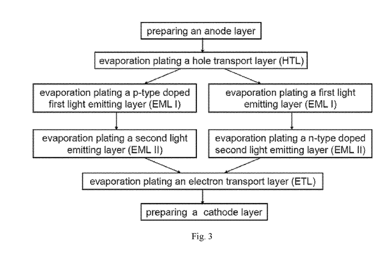
[0059]1) Sputtering an anode conductive film on a substrate. If the organic electroluminescent device is a top-emitting device, the anode layer can be made of a reflective material. If the organic electroluminescent device is a bottom-emitting device, the anode layer can be made of a transparent material; the material of the anode layer can be ITO (In2O3:SnO2), IZO (In2O3:ZnO), GITO (Ga0.08In0.28Sn0.64O3), or ZITO (Zn0.64In0.88Sn0.66O3);

[0060]2) After preparing the anode conductive film, preparing a hole transport layer (HTL) with vacuum evaporation process. Optionally, a material with a high hole mobility is used as the hole transport layer; a material of the hole transport layer can be N,N′-bis(1-naphthalenyl)-N,N′-diphenyl-1,1′-biphenyl-4,4′-diamine (NPB), triphenyl-diamine derivative (TPD), N,N′-bis(phenyl)-N,N′-bis(4′-(N,N-bis(phenylamino)-4-biphenyl)benzidine (TPTE), or 1,3,5-tris(N-3-methylphenyl-N-phenylamino)benzene (TDAB), etc.;

[0061]3) Preparing a first light emitting lay...

example 2

[0065]1) Sputtering an anode conductive film on a substrate. If the organic electroluminescent device is a top-emitting device, the anode layer can be made of a reflective material. If the organic electroluminescent device is a bottom-emitting device, the anode layer can be made of a transparent material. The material of the anode layer can be ITO (In2O3:SnO2), IZO (In2O3:ZnO), GITO (Ga0.08In0.28Sn0.64O3), or ZITO (Zn0.64In0.88Sn0.66O3);

[0066]2) After preparing the anode conductive film, preparing a hole transport layer (HTL) with vacuum evaporation process. Optionally, a material with a high hole mobility is used as the hole transport layer. A material of the hole transport layer can be N,N′-bis(1-naphthalenyl)-N,N′-diphenyl-1,1′-biphenyl-4,4′-diamine (NPB), triphenyl-diamine derivative (TPD), N,N′-bis(phenyl)-N,N′-bis(4′-(N,N-bis(phenylamino)-4-biphenyl)benzidine (TPTE), or 1,3,5-tris(N-3-methylphenyl-N-phenylamino)benzene (TDAB), etc.;

[0067]3) Preparing a first light emitting lay...


PUM


Abstract

The embodiments of the present invention provide an organic electroluminescent device, a manufacturing method thereof and an electronic equipment. The organic electroluminescent device comprises: an anode layer, a hole transport layer, a first light emitting layer, a second light emitting layer, an electron transport layer, and a cathode layer stacked in sequence; wherein the first light emitting layer and the second light emitting layer comprise a same substrate material; the first light emitting layer and / or the second light emitting layer are doped such that a hole mobility of the first light emitting layer is equal to an electron mobility of the second light emitting layer. In the embodiments of the present invention, two light emitting layers with the same substrate material are applied, which can realize a balanced injection for electrons and holes, thereby improving the efficiency and lifetime of the organic electroluminescent device.

Description

RELATED APPLICATIONS[0001]The present application is the U.S. national phase entry of PCT / CN2015 / 087775, with an international filing date of Aug. 21, 2015, which claims the benefit of Chinese Patent Application No. 201510180124.7, filed on Apr. 16, 2015, the entire disclosures of which are incorporated herein by reference.FIELD OF THE INVENTION[0002]The present invention relates to the field of display technology, particularly to an organic electroluminescent device, a manufacturing method thereof and an electronic equipment.BACKGROUND OF THE INVENTION[0003]Organic electroluminescent devices (OLED) are highly valued in flat panel display and lighting fields due to the advantages of high brightness, color saturation, thin and light, flexible and so on. At present, a common organic electroluminescent device mainly comprises top-emitting device structure and bottom-emitting device structure. Compared with the bottom-emitting device structure, the top-emitting device structure has adva...

Claims


Application Information

Patent Timeline
IPC IPC(8): H01L51/00C09K11/06
CPCH01L51/0072H01L2051/0063H01L51/005H01L51/0081H01L51/0054H01L51/0059C09K11/06H01L51/006H01L51/0077H01L51/0084H01L51/0086H01L51/007H01L51/0067H01L51/56H01L51/5056H01L51/5072H01L51/5206H01L51/5221H01L51/5012H01L51/504H01L2251/305H01L2251/306H01L2251/308H01L2251/301C09K2211/1007C09K2211/1014H01L51/0058C09K2211/1011C09K2211/181C09K2211/188C09K2211/185H01L51/0065H10K85/631H10K85/30H10K50/11H10K50/12H10K50/13H10K71/00H10K50/81H10K50/82H10K71/164C09K2211/1029H10K85/6572H10K85/60H10K85/324H10K85/341H10K85/344H10K85/622H10K85/633H10K85/653H10K85/654H10K85/6565H10K50/15H10K50/16H10K85/626H10K2102/00H10K2102/101H10K2102/102H10K2102/103
Inventor WU, HAIDONGQIU, YUNLAI, WEILIN
Owner BOE TECH GRP CO LTD
Learn More