Manufacturing method of display device and display device

a display device and manufacturing method technology, applied in the direction of basic electric elements, semiconductor devices, electrical equipment, etc., can solve the problems of deterioration of organic film properties, increased cost of eliminating organic film, and deterioration of display device quality

Active Publication Date: 2017-05-11
JAPAN DISPLAY INC
View PDF4 Cites 20 Cited by
  • Summary
  • Abstract
  • Description
  • Claims
  • Application Information

AI Technical Summary

Benefits of technology

[0008]Water and oxygen may enter from a frame area of the display device, pass through the inside of an organic film formed over a display area and the frame area, and thus reach the display area. Therefore, a structure in which the organic film around the display area is eliminated to prevent the entry of water and oxygen into the organic film formed in the display area may be employed.

Problems solved by technology

In that case, the laser irradiation area increases according to the size of the display area and therefore the cost of eliminating the organic film increases.
Also, as the laser irradiation area increases, properties of the organic film may deteriorate due to heat from the irradiation, and the quality of the display device may deteriorate due to the scattering of the eliminated organic film.

Method used


Image

  • Manufacturing method of display device and display device
  • Manufacturing method of display device and display device
  • Manufacturing method of display device and display device

Examples


Embodiment Construction

[0037]Hereinafter, each embodiment of the invention will be described with reference to the drawings. However, the disclosure is only an example, and as a matter of course, any change that can be easily thought of by a person skilled in the art without departing from the spirit of the invention should be included in the scope of the invention. In order to clarify the explanation, the drawings may schemaitcally show each part in terms of its width, thickness, shape and the like, compared with the actual Configuration. However, this is simply an example and should not limit the interpretation of the invention. Also, elements similar to those described before with reference to already mentioned drawings may be denoted by the same reference signs, and detailed description of these elements may be omitted when appropriate.

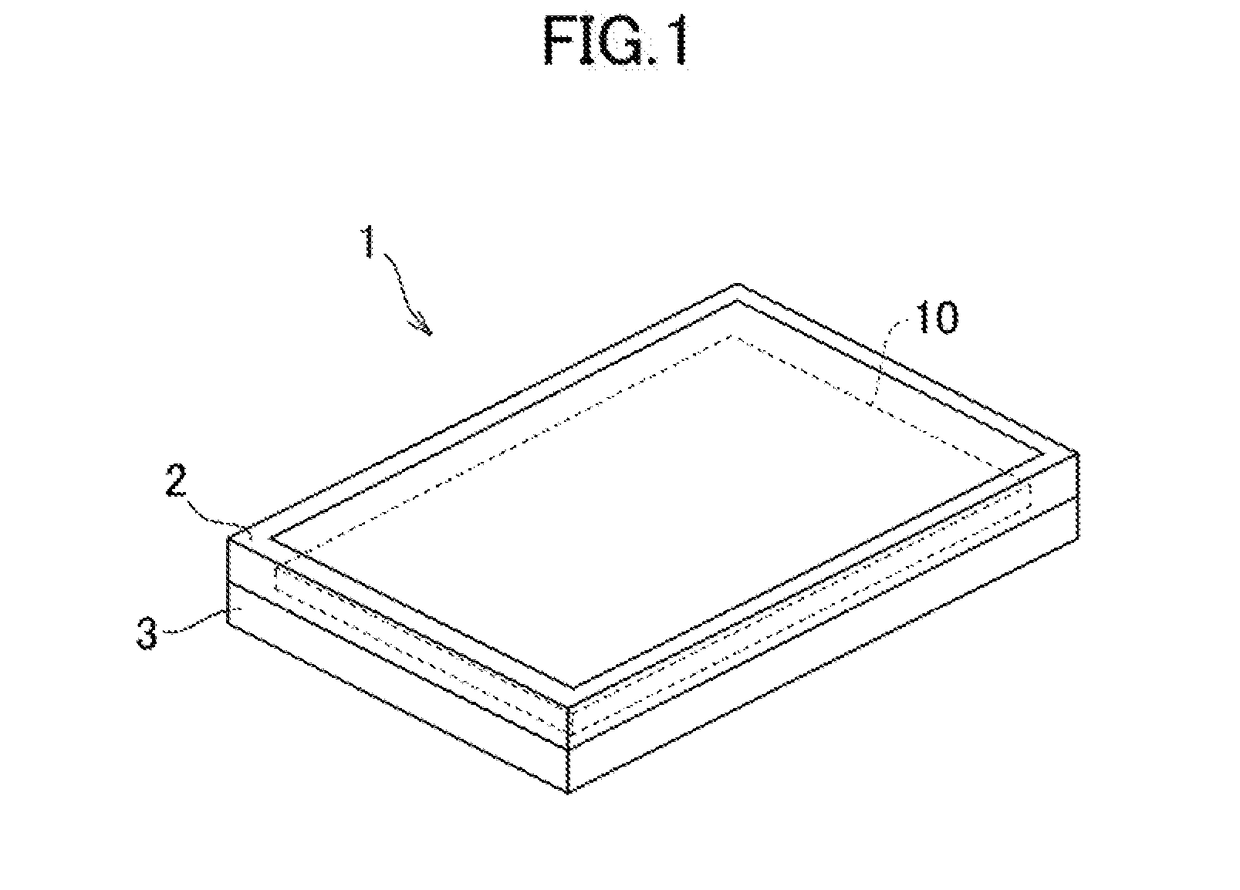
[0038]FIG. 1 is a perspective view showing a display device 1 according to an embodiment of the invention. The display device 1 includes a display panel 10 fixed in suc...


PUM


Abstract

A manufacturing method of a display device includes: forming, in a resin layer including a display area where a plurality of lower electrodes is formed and a peripheral area surrounding the display area, a band-like groove which divides the resin layer in a form of surrounding the display area; forming an organic electroluminescence layer including a light emitting layer, on the resin layer and inside the band-like groove in such a way as to be placed on the plurality of lower electrodes; irradiating the organic electroluminescence layer with a pulse laser and thus eliminating the organic electroluminescence layer in such a way that a part of the organic electroluminescence layer is left in a shape of an island at least on a bottom surface of the band-like groove and that the bottom surface of the band-like groove is continuously exposed in the form of surrounding the display area.

Description

CROSS-REFERENCE TO RELATED APPLICATION[0001]The present application claims priority from Japanese application JP2015-217895 filed on Nov. 5, 2015, the content of which is hereby incorporated by reference into this application.BACKGROUND OF THE INVENTION[0002]1. Field of the Invention[0003]The present invention relates to a manufacturing method of a display device and a display device.[0004]2. Description of the Related Art[0005]In a display device such as an organic EL (electroluminescence) display device, a self-light emitting element such as an organic light emitting diode (OLED) may be controlled using a switching element such as a transistor, thus displaying an image. Here, an organic material used for the organic light emitting diode may react with water and oxygen and thus deteriorate. Therefore, the organic EL panel may be sealed so that the organic material will not be exposed to the outside air.[0006]JP2006-392860A discloses an EL element which includes an organic material ...

Claims


Application Information

Patent Timeline
Patent Type & Authority Applications(United States)
IPC IPC(8): H01L51/00H01L51/52
CPCH01L51/0018H01L51/5253H01L51/5012H01L2227/323H01L27/3258H01L27/3246H01L51/5237H10K59/124H10K71/233H10K50/844H10K59/87H10K50/11H10K50/84H10K59/122H10K59/1201
Inventor MIMURA, TOSHIFUMIWATABE, MASAHIROSATO, TOSHIHIRO
Owner JAPAN DISPLAY INC
Why Eureka
Try Eureka