
Wafer image inspection apparatus

Active Publication Date: 2017-01-05
NEXTIN +1
View PDF12 Cites 10 Cited by
  • Summary
  • Abstract
  • Description
  • Claims
  • Application Information

AI Technical Summary

Benefits of technology

The present invention allows for the creation of multiple images with different focal positions by using a split optical element and controlling the distance between the focusing optical system and image pick-up elements. This allows for the inspection of three-dimensional fine patterns for defects, using a processing apparatus.

Problems solved by technology

However, to photograph a field of view to be photographed which has been radiated by lighting using a single image pick-up element requires a very long time taken to inspect the entire wafer because an existing image pick-up element has a limited capacity.
Although a high-capacity image pick-up element is used, it is not appropriate because a lot of time is taken by a computer system connected to the image pick-up element and analyzing an image.
In the focal plane array, however, it is practically difficult to dispose a plurality of unit image pick-up elements closely.
If we take such a lead wire installation space into consideration, it is hard to think that the pixel areas of the plurality of image pick-up elements are closely disposed in a matrix form.
However, as the degree of integration of devices is increased, it has become difficult to reduce the size of the devices and wires due to several limits in terms of a process for fabricating the semiconductor apparatus, for example, the optical limit of a photolithography process.
Furthermore, to reduce the size of the devices has reached the state in which a device function may be problematic.
The three-dimensional configuration of semiconductor apparatuses has a problem in that an inspection cannot be performed sufficiently and properly using a conventional plane inspection method for the semiconductor apparatus.
If patterns are too small, it is difficult for a lighting beam to reach the patterns through the patterns.
Such a method has many difficulties in measuring a new three-dimensional structure of semiconductor apparatuses.
It is difficult to use a non-optical image processing method, such as a scanning probe microscopy, as a practical inspection apparatus because the scanning probe microscopy is expensive and slow.
However, to obtain optical images having many different focal positions with respect to a very small object is a task requiring a lot of time.
A method which solves problems and which is substantially used for the illumination of a semiconductor apparatus has not yet been properly proposed.

Method used


Image

  • Wafer image inspection apparatus
  • Wafer image inspection apparatus
  • Wafer image inspection apparatus

Examples


Embodiment Construction

[0047]Hereinafter, the present invention is described in more detail in connection with embodiment with reference to the accompanying drawings.

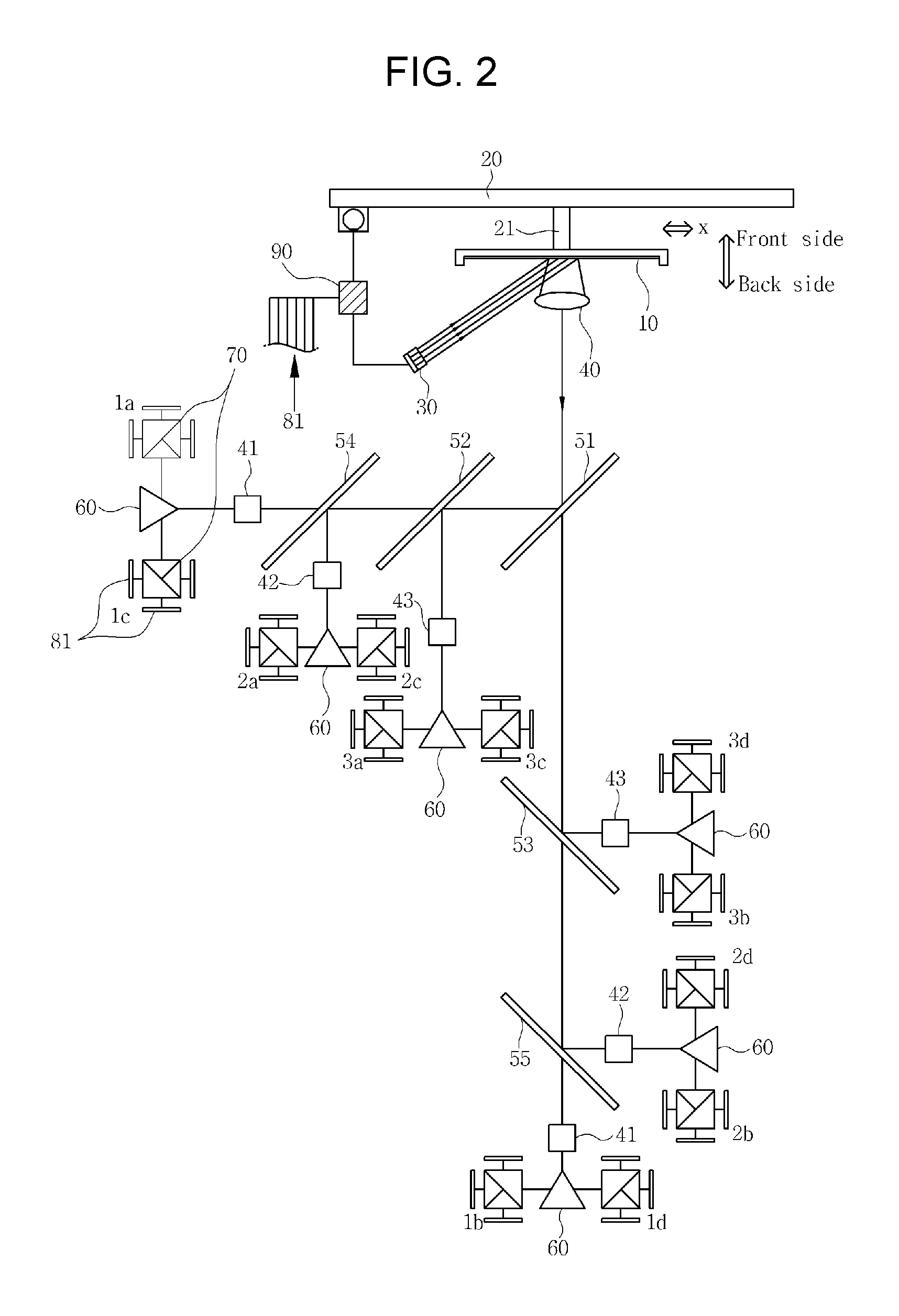
[0048]FIG. 2 is a conceptual diagram simplifying and schematically showing the configuration of major elements of the present invention.

[0049]A configuration of a wafer image inspection apparatus according to the present invention is described through the present embodiment. A wafer 10 has been held by the wafer fixing chuck 21 of a wafer stage 20 or wafer movement stage and may move in the x-axis and y-axis directions on a plane parallel to the plane of the wafer. In this case, the wafer 10 consecutively moves in the x direction of an arrow. Such a wafer stage has been used as substantially the same method in several pieces of equipment for wafer processing, and a detailed configuration thereof is omitted.

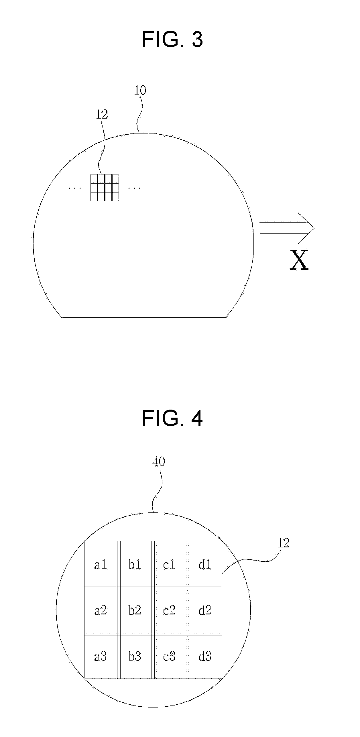
[0050]FIG. 3 shows a field of view to be photographed, which is photographed once on the wafer 10 and includes a 3×4 matrix of unit areas ...


PUM


Abstract

ProA wafer image inspection apparatus for inspecting defects of a semiconductor wafer comprises: a lighting portion for generating light; a lens portion for obtaining a wafer image, which is reflected after the light has been reflected onto a wafer to be inspected, and delivering the wafer image by lighting same in one direction; a dividing optical element for dividing the wafer image delivered from the lens portion; an image detection portion comprising a plurality of image-capturing elements, which are installed so that images which have passed through the lens portion and the dividing optical element are respectively formed on different focus positions; and an image processing portion for combining the images on different focus positions captured by the plurality of image pick-up elements to form a TSOM image, and comparing the TSOM image with a TSOM image of a normal semiconductor apparatus part to determine whether an object is defective.

Description

TECHNICAL FIELD[0001]The present invention relates to a wafer inspection apparatus and, more particularly, to a wafer inspection apparatus capable of obtaining an image of a wafer part in which a semiconductor circuit has been formed, analyzing the image, and inspecting whether a defect is present in the wafer part.BACKGROUND ART[0002]In a wafer inspection apparatus for obtaining an image of a portion of a wafer and inspecting the image, in general, lighting having a single wavelength pulse is radiated to a corresponding area of the wafer while the wafer passes through a predetermined area for photographing(capturing image). Furthermore, a field of view (FOV) in which a lens unit may obtain an image is illuminated through a single piece of pulse lighting. Reflected light from the field of view passes through the lens unit, and an image of the photographing area (object area) of the wafer is focused on the pixel unit of an image pick-up element which functions as a screen at the back...

Claims


Application Information

Patent Timeline
IPC IPC(8): G01N21/88G01N21/95
CPCG01N21/9501H01L22/12G01N21/8806G01N21/8851G01N2021/8887G01N2201/063
Inventor PARK, TAE HOONRAM, SEGAL
Owner NEXTIN
Learn More