Transparent nanowire electrode comprising a functional organic layer
a functional organic layer and transparent technology, applied in the direction of organic semiconductor devices, non-conductive materials with dispersed conductive materials, metal/alloy conductors, etc., can solve the problems of heat acting on the electrode, the resistance of the sheet is particularly large, and the flexibility electrodes available at the moment cannot meet all the requirements at the same time, so as to reduce the problem of further processing the electrode and increase the adhesion of the conductive layer
- Summary
- Abstract
- Description
- Claims
- Application Information
AI Technical Summary
Benefits of technology
Problems solved by technology
Method used
Image
Examples
first embodiment
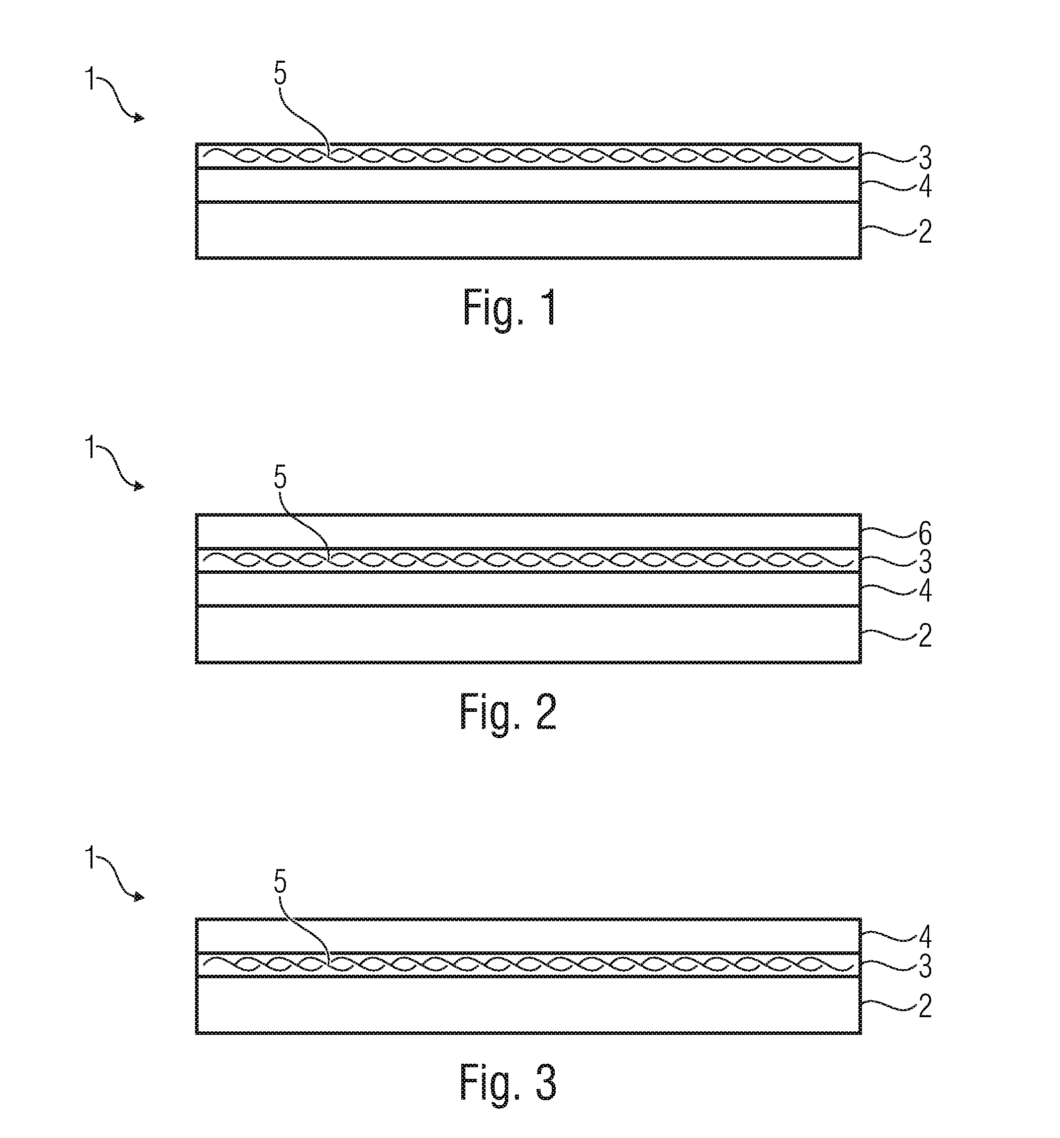
[0061]FIG. 1 shows an inventive flexible and transparent electrode 1 in a schematic side view. The transparent electrode 1 comprises at least one carrier layer 2 for stabilizing the electrode 1, at least one electrically conductive layer 3 containing metal nanowires 5, which is produced by spreading a suspension of a liquid and the metal nanowires 5 surrounded by a stabilizing layer, along the carrier layer 2 and solidifying same by removing the liquid, and at least one functional organic layer 4 formed along the carrier layer 2, which, while the electrically conductive layer 3 solidifies, by means of an electrical interaction with the metal nanowires 5 and / or with the stabilizing layers of the metal nanowires 5, changes an interaction between the metal nanowires 5 and the stabilizing layers such that the result is a substance-to-substance bond between the metal nanowires 5.
[0062]In accordance with a further development of the invention, the organic layer 4 is formed between the car...
second embodiment
[0064]FIG. 2 shows an inventive flexible and transparent electrode in a schematic side view. In accordance with a further development of the invention shown here, the electrically conductive layer 3 is provided with a transparent cover layer 6 on a side facing away from the organic layer 4. This reduces unevenness resulting from the nanowires 5 and thus reduces problems when further processing the electrode.
third embodiment
[0065]FIG. 3 shows an inventive flexible and transparent electrode in a schematic side view. In accordance with a further embodiment of the invention shown here, the organic layer 4 is formed on that side of the electrically conductive layer 3 facing away from the carrier layer 2. In this case, a producing method is made possible in which at first the carrier layer 2 is provided, then the electrically conductive layer 3 is applied directly or indirectly onto the carrier layer 2 and, after that, the organic layer 4 is formed on the electrically conductive layer 3. In such embodiments, it is of advantage for the electrically conductive layer 3 to be applied directly onto the carrier layer 2. However, it is also possible to provide further layers between the carrier layer 2 and the electrically conductive layer 3. An adhesion promoting layer for increasing adhesion between the conductive layer 2 and the carrier layer 2 may, for example, be provided.
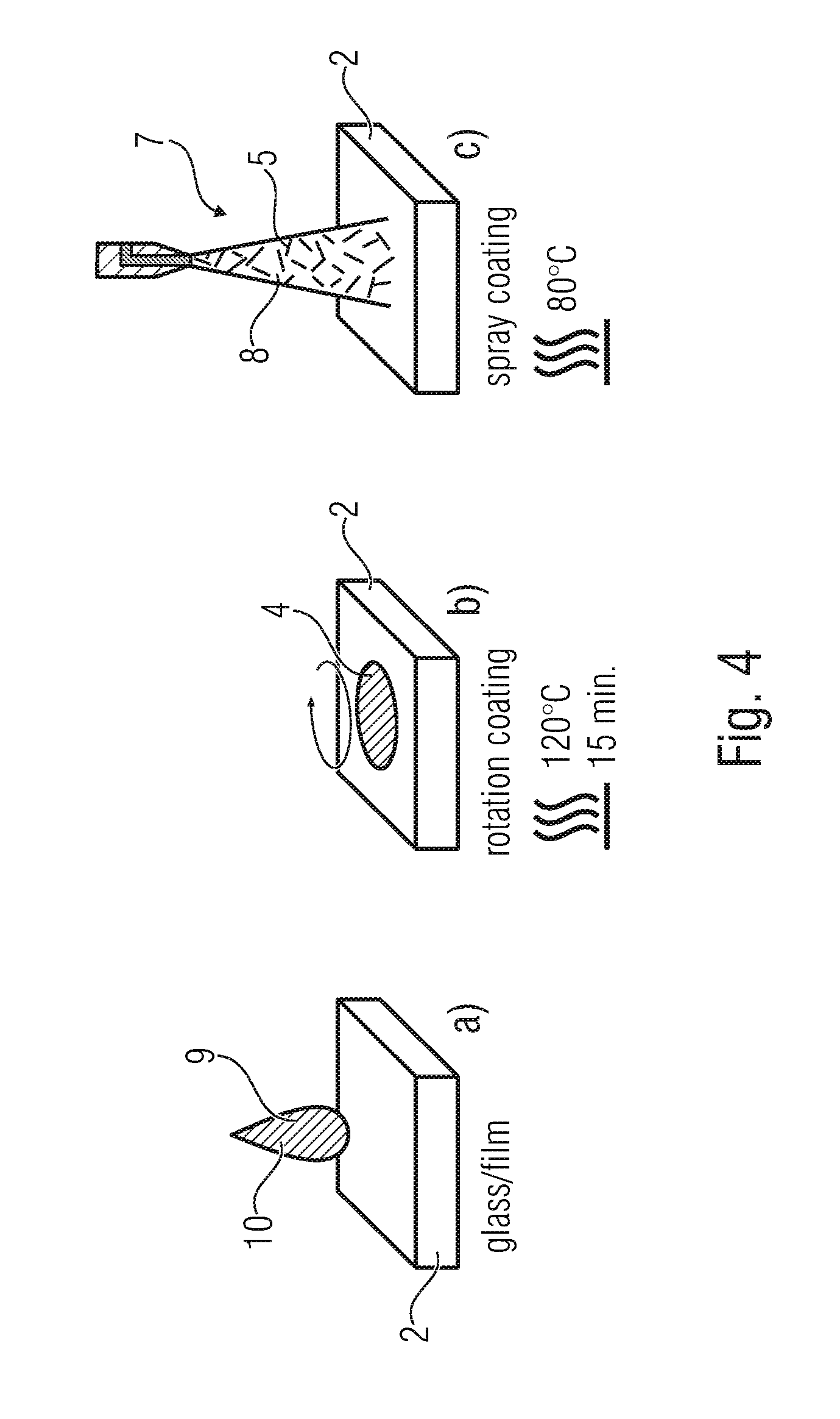
[0066]FIG. 4 shows an embodiment of a...
PUM
| Property | Measurement | Unit |
|---|---|---|
| temperature | aaaaa | aaaaa |
| temperature | aaaaa | aaaaa |
| temperature | aaaaa | aaaaa |
Abstract
Description
Claims
Application Information
 - R&D
- Intellectual Property
- Life Sciences
- Materials
- Tech Scout
- Unparalleled Data Quality
- Higher Quality Content
- 60% Fewer Hallucinations
Browse by: Latest US Patents, China's latest patents, Technical Efficacy Thesaurus, Application Domain, Technology Topic, Popular Technical Reports.
© 2025 PatSnap. All rights reserved.Legal|Privacy policy|Modern Slavery Act Transparency Statement|Sitemap|About US| Contact US: help@patsnap.com


