NAND String Utilizing Floating Body Memory Cell

a floating body memory and nand string technology, applied in the direction of semiconductor/solid-state device details, digital storage, instruments, etc., can solve the problems of major complication, data loss of static random access memory (sram) and dynamic random access memory (dram)

Active Publication Date: 2016-09-15
ZENO SEMICON
View PDF4 Cites 35 Cited by
  • Summary
  • Abstract
  • Description
  • Claims
  • Application Information

AI Technical Summary

Benefits of technology

The present invention provides a NAND string configuration and a semiconductor memory array that includes a plurality of semiconductor memory cells connected in a string of semiconductor memory cells. The NAND string configuration includes a select gate drain device and a select gate source device connected to either end of the string of semiconductor memory cells. The semiconductor memory cells each include a floating body region that can be charged to a level indicative of a state of the memory cell. The semiconductor memory cell can be made using a fin structure that extends vertically above an insulator layer. The technical effects of the invention include a more efficient and compact memory cell configuration, improved data storage and retrieval, and better cell performance.

Problems solved by technology

Volatile memory devices such as static random access memory (SRAM) and dynamic random access memory (DRAM) lose data that is stored therein when power is not continuously supplied thereto.
This is often a major complication for arrays configured in the NOR orientation since they all share a single electrically connected bit line.

Method used


Image

  • NAND String Utilizing Floating Body Memory Cell
  • NAND String Utilizing Floating Body Memory Cell
  • NAND String Utilizing Floating Body Memory Cell

Examples


Embodiment Construction

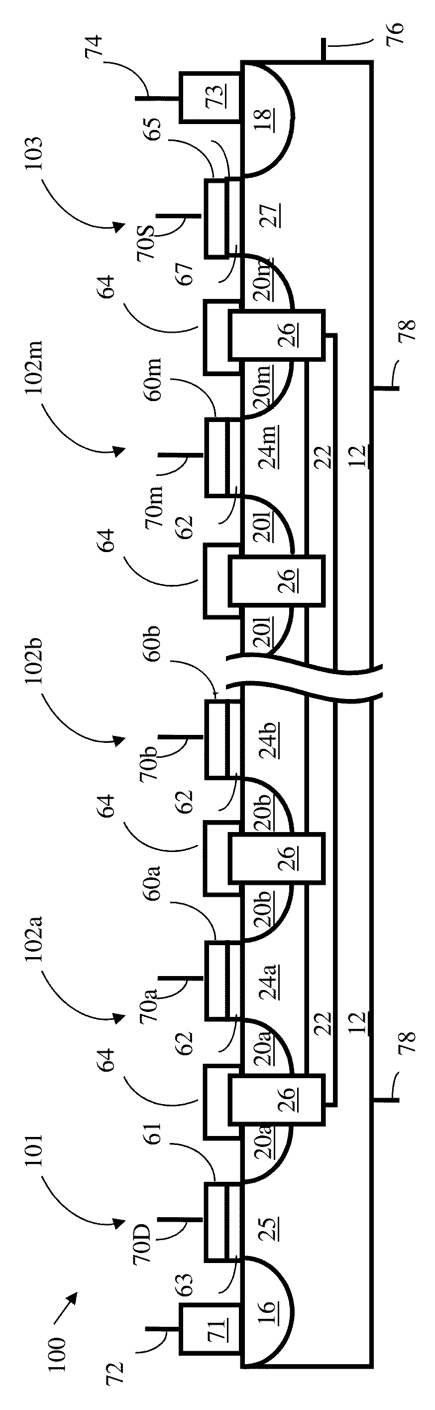
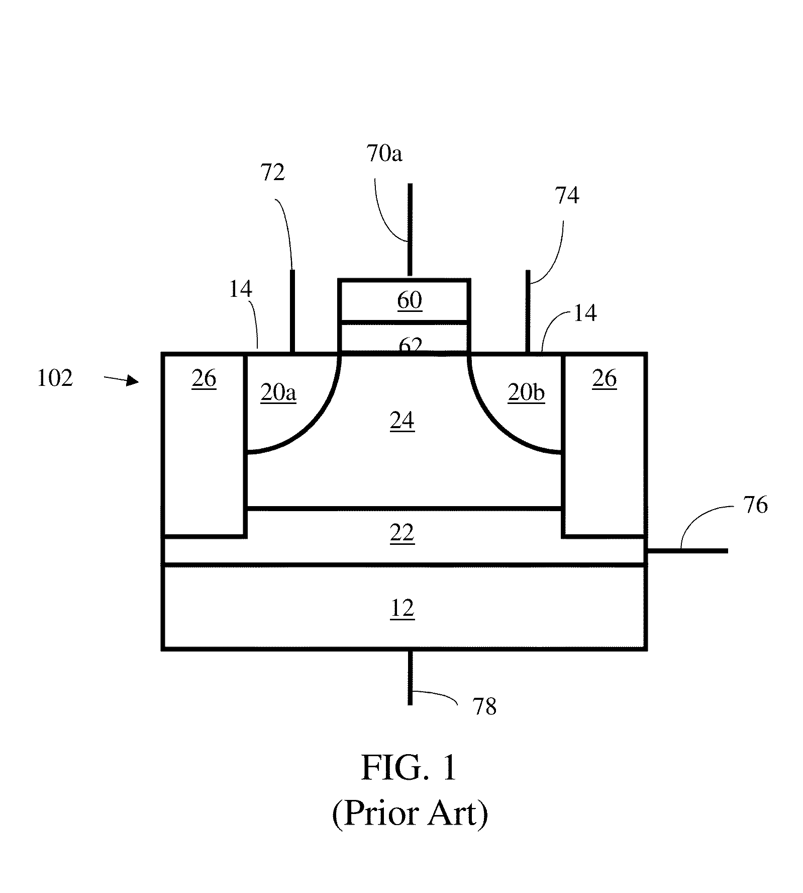
[0080]Before the present memory cells, strings, arrays and methods are described, it is to be understood that this invention is not limited to particular embodiments described, as such may, of course, vary. It is also to be understood that the terminology used herein is for the purpose of describing particular embodiments only, and is not intended to be limiting, since the scope of the present invention will be limited only by the appended claims.

[0081]Where a range of values is provided, it is understood that each intervening value, to the tenth of the unit of the lower limit unless the context clearly dictates otherwise, between the upper and lower limits of that range is also specifically disclosed. Each smaller range between any stated value or intervening value in a stated range and any other stated or intervening value in that stated range is encompassed within the invention. The upper and lower limits of these smaller ranges may independently be included or excluded in the ra...


PUM


Abstract

NAND string configurations and semiconductor memory arrays that include such NAND string configurations are provided. Methods of making semiconductor memory cells used in NAND string configurations are also described.

Description

CROSS-REFERENCE[0001]This application claims the benefit of U.S. Provisional Application No. 61 / 818,305, filed on May 1, 2013 and of U.S. Provisional Application No. 61 / 829,262, filed on May 31, 2013, both of which application are hereby incorporated herein, in their entireties, by reference thereto.FIELD OF THE INVENTION[0002]The present invention relates to semiconductor memory technology. More specifically, the invention relates to a semiconductor device utilizing an electrically floating body transistor.BACKGROUND OF THE INVENTION[0003]Semiconductor memory devices are used extensively to store data. Memory devices can be characterized according to two general types: volatile and non-volatile. Volatile memory devices such as static random access memory (SRAM) and dynamic random access memory (DRAM) lose data that is stored therein when power is not continuously supplied thereto.[0004]A DRAM cell without a capacitor has been investigated previously. Such memory eliminates the capa...

Claims


Application Information

Patent Timeline
Patent Type & Authority Applications(United States)
IPC IPC(8): G11C16/04H01L27/088H01L21/265H01L23/528G11C5/06H01L27/115H01L29/78
CPCG11C16/0483H01L27/11524H01L27/1157H01L21/26586H01L29/7841H01L23/528G11C5/063H01L27/0886H01L29/66659G11C16/0416H10B69/00H10B12/20H10B12/50H10B41/35H10B43/35G11C11/4096G11C11/4099G11C2211/4016H01L29/1087H01L29/1095H01L29/785
Inventor LOUIE, BENJAMIN S.HAN, JIN-WOOWIDJAJA, YUNIARTO
Owner ZENO SEMICON
Why Eureka
Try Eureka