Symmetric target design in scatterometry overlay metrology
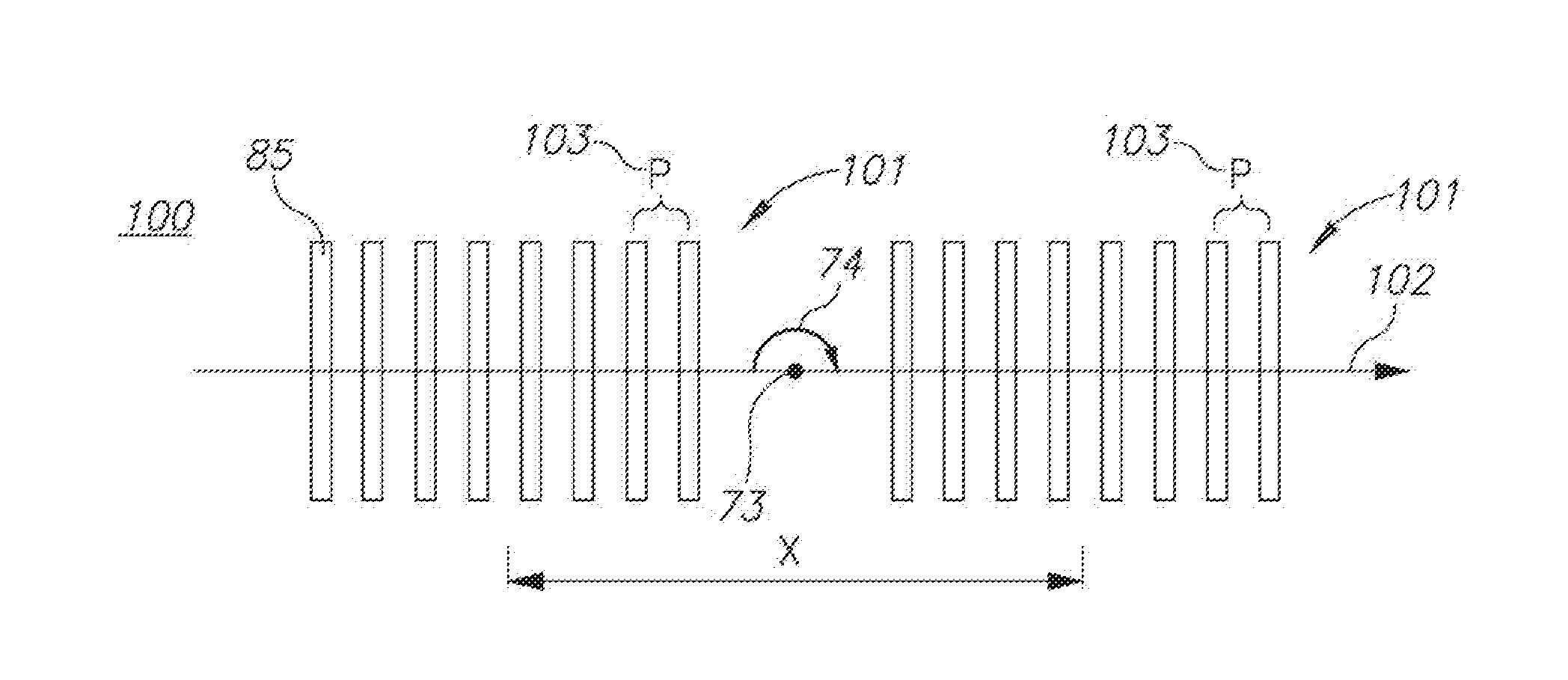
a scatterometry overlay and target technology, applied in the field of metalrology of semiconductor devices, can solve the problems of low overlay sensitivity, increased target real-estate, and increased coo (cost of ownership) of the metrology tool,
- Summary
- Abstract
- Description
- Claims
- Application Information
AI Technical Summary
Benefits of technology
Problems solved by technology
Method used
Image
Examples
example 1
Multiple Measurements
[0124]In certain embodiments, method 500 comprises setting the illumination beams to exhibit no phase differences (stage 510) i.e. setting φ1,2=0; illuminating separately each periodic structure to measure the respective diffracted intensity (stage 512), i.e. illuminating grating (1) alone to provides a measurement of |En(1)({right arrow over (k)})| and illuminating grating (2) alone to provides a measurement of |En(2)({right arrow over (k)}) (e.g. by turning off the beams illuminating the other grating respectively); illuminating simultaneously the periodic structures to measure the interference term (stage 514) of Equation 4 and extracting the overlay from interference measurements for ±1 diffraction orders and opposite locations ±k (stage 516).
[0125]For example, stage 516 may be carried out as follows: Extracting the cosine
Cn(k→)=cos(2π·(OVL+Offset)·nPitch+ψn(1)(k→)-ψn(2)(k→)+k→·X→)
for each order n=+1, n=−1. From the cosines, extracting the two mathematically...
example 2
Compensated Field Shifts
[0131]In certain embodiments, method 500 comprises setting the illumination beams to exhibit no phase differences (stage 510) i.e. setting φ1,2=0; imaging the wafer to a field conjugate plane (stage 530) and performing image shifting at the field conjugate plane (stage 532), e.g. by modifying the image to shift the image part containing one of the gratings in the direction of the grating by N different shifts, with N≧3, compensating for the image shifting in the illumination (stage 534) and extracting the overlay algorithmically from the compensated image shifts (stage 536).
[0132]The following non-limiting example illustrates the method with N=4 and
Offseta=Pitch4a,
with a=0,1,2, and 3. As the generalization to N=3 and N≧5 is straightforward the following calculated can be easily adjusted.
[0133]Image shifting 532 may be compensated by shifting the illuminating beam in an opposite direction, to maintain the overall position of the image unchanged (stage 534). Fo...
example 3
Wafer Shifts
[0148]In certain embodiments, method 500 comprises performing image shifts physically (stage 538) and extracting the overlay algorithmically along principles similar to the ones described in Example 2. Generally, physical image shift, carried out by moving the wafer, may replace all or some of the N signals described above. In certain embodiments, images of each side-by-side cell couple may be taken once, without any spot compensation procedure.
PUM
| Property | Measurement | Unit |
|---|---|---|
| periodic structure | aaaaa | aaaaa |
| periodic structures | aaaaa | aaaaa |
| size | aaaaa | aaaaa |
Abstract
Description
Claims
Application Information
 - R&D
- Intellectual Property
- Life Sciences
- Materials
- Tech Scout
- Unparalleled Data Quality
- Higher Quality Content
- 60% Fewer Hallucinations
Browse by: Latest US Patents, China's latest patents, Technical Efficacy Thesaurus, Application Domain, Technology Topic, Popular Technical Reports.
© 2025 PatSnap. All rights reserved.Legal|Privacy policy|Modern Slavery Act Transparency Statement|Sitemap|About US| Contact US: help@patsnap.com


