Organic light emitting display device and manufacturing method therof

Active Publication Date: 2016-06-30
LG DISPLAY CO LTD
View PDF4 Cites 12 Cited by
  • Summary
  • Abstract
  • Description
  • Claims
  • Application Information

AI Technical Summary

Benefits of technology

The present invention provides an OLED device and a manufacturing method that addresses limitations and disadvantages of existing technologies. The invention aims to prevent pile-up issues without reducing the size of the emitting area. The OLED device includes a thin film transistor, a planarization layer, a first bank layer, a lower electrode, an organic emitting layer, and an upper electrode. This structure allows for improved manufacturing and reduced pile-up issues, resulting in a more efficient and effective OLED device.

Problems solved by technology

When the organic emitting layer 14 is formed by a wet process, a pile-up problem is generated in the organic emitting layer 14.
However, the OLED device including the double-layered bank layer has is limited due to a decreased size of the emitting area resulting from a process margin for overlapping the lower electrode 24, the lower bank layer 22 and the upper bank layer 23.

Method used


Image

  • Organic light emitting display device and manufacturing method therof
  • Organic light emitting display device and manufacturing method therof
  • Organic light emitting display device and manufacturing method therof

Examples


Embodiment Construction

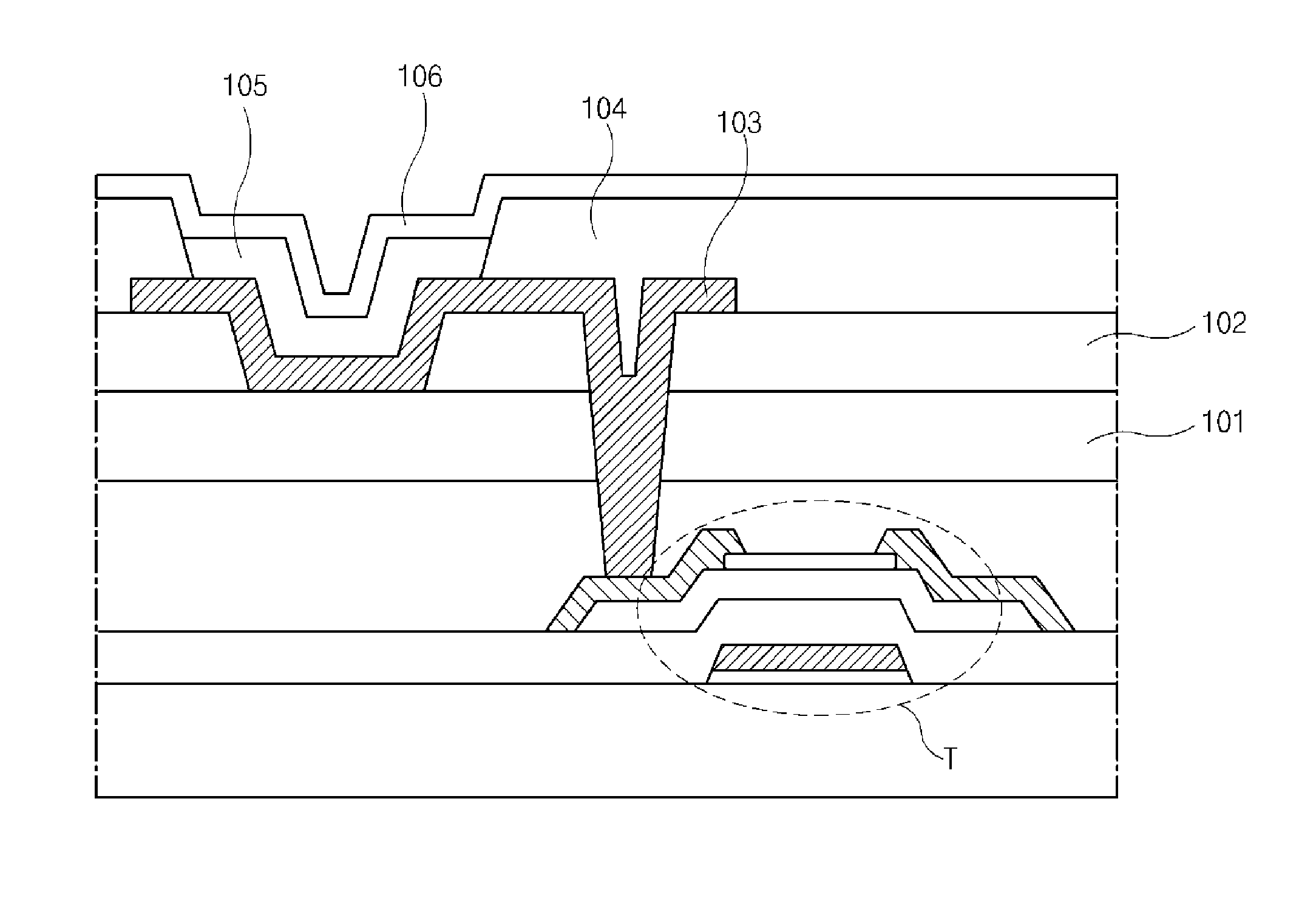
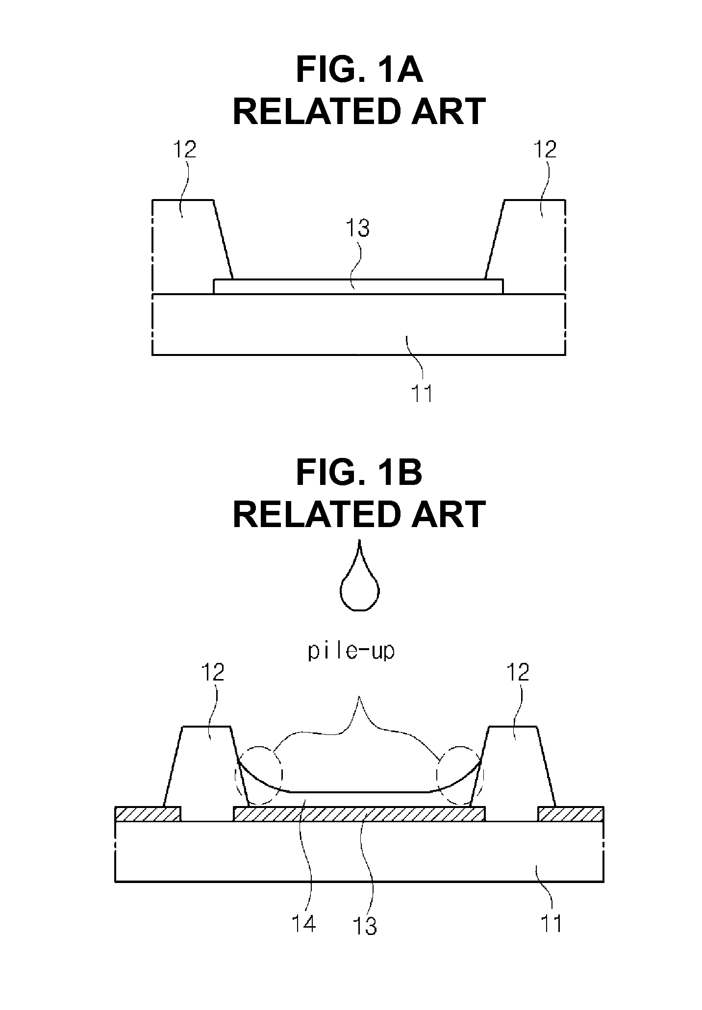
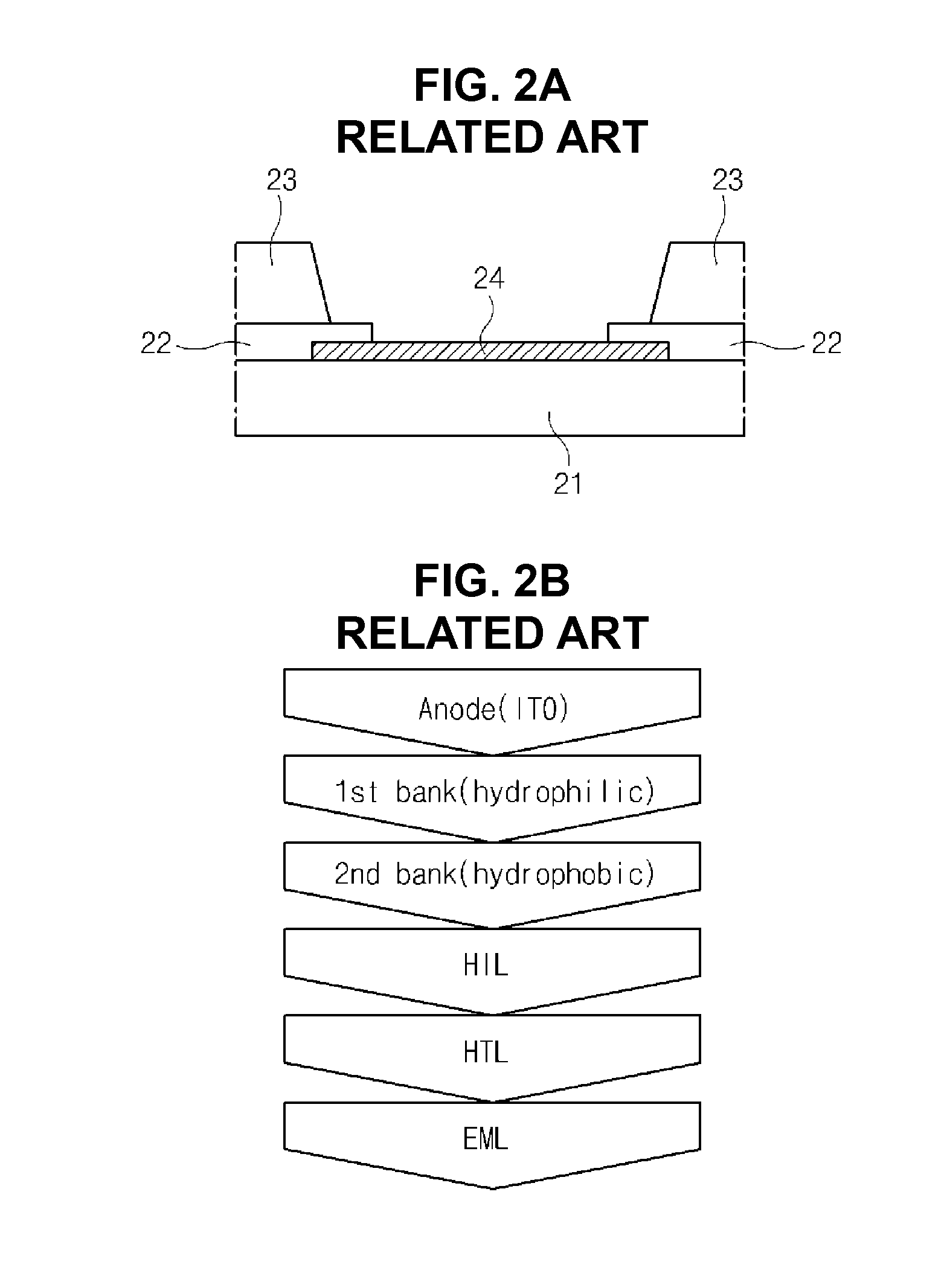
[0025]The present invention will be embodied in many different forms and is not limited to the embodiments set forth herein. Rather, these embodiments are provided to complete the disclosure of the present invention and completely convey the concept of the invention to one of skill in the art. In addition, elements of the embodiments of the present invention as disclosed below can be combined with each other, and the combination of the elements belongs to a scope of the present invention.

[0026]Shapes, sizes, rates, angles, numbers, etc. as disclosed in the drawings for explaining the embodiments of the present invention are illustrative and are not limited to the details shown. Wherever possible, the same reference numerals throughout the specification refer to the same or like parts. Additionally, in the following description of embodiments of the present invention, a detailed description of the well-known technique that is determined to unnecessarily obscure the subject matter of ...


PUM


Abstract

An organic light emitting display (OLED) device, and a method for manufacturing the OLED device are discussed. The OLED device according to one embodiment includes a thin film transistor formed on a substrate; a planarization layer formed on the thin film transistor; a first bank layer including a first opening; a lower electrode formed in the first opening and connected to the thin film transistor, an end segment of the lower electrode being disposed on the first bank layer; a second bank layer formed on the first bank layer and covering the end segment of the lower electrode, the second bank layer including a second opening corresponding to the first opening; an organic emitting layer formed on the lower electrode and in the second opening; and an upper electrode formed on the organic emitting layer.

Description

CROSS REFERENCE TO RELATED APPLICATIONS[0001]The present application claims the benefit of Korean Patent Application No. 10-2014-0195136 filed in Korea on Dec. 31, 2014, the contents of which are hereby incorporated by reference in their entirety.BACKGROUND OF THE INVENTION[0002]1. Field of the Disclosure[0003]The present invention relates to an organic light emitting display (OLED) device capable of preventing a pile-up problem and a manufacturing method thereof.[0004]2. Description of the Related Art[0005]Flat display devices having a thin profile, light weight, low power consumption and high display quality include a liquid crystal display (LCD) device, a plasma display panel (PDP) and an OLED device. The OLED device is self-emitting and does not require an additional light source. As a result, the OLED device can be thinner and lighter weight and have a faster response time, improved color reproduction, lower power consumption, improved viewing angle, etc. Generally, the OLED de...

Claims


Application Information

Patent Timeline
IPC IPC(8): H01L27/32H01L51/50H01L51/00H01L51/56
CPCH01L27/3246H01L27/3258H01L51/56H01L2227/323H01L51/0005H01L2251/558H01L51/5012H10K59/122H10K59/84H10K59/00H10K71/00H10K71/135
Inventor PARK, HONG-KIBAE, HYO-DAEKIM, SOO-JIN
Owner LG DISPLAY CO LTD
Why Eureka
Try Eureka