Chip package and method for forming the same

a chip and packaging technology, applied in the field of chip package technology, can solve the problems of poor conductance between the signal contact pad and the conducting layer, insufficient structural strength, and negative impact on the quality of such chip packages

Active Publication Date: 2016-06-23
XINTEC INC
View PDF3 Cites 12 Cited by
  • Summary
  • Abstract
  • Description
  • Claims
  • Application Information

AI Technical Summary

Benefits of technology

The invention is about a structure called a redistribution layer that enhances the connection between a semiconductor chip and external circuits. The redistribution layer penetrates through conducting pads and is embedded within them, making them stronger and more reliable. This improves the quality and reliability of the chip packages.

Problems solved by technology

However, conductance between the signal contact pad and the conducting layer is poor.
Also, structural strength is insufficient.
As a result, the quality of such chip packages is negatively affected.

Method used


Image

  • Chip package and method for forming the same
  • Chip package and method for forming the same
  • Chip package and method for forming the same

Examples


Embodiment Construction

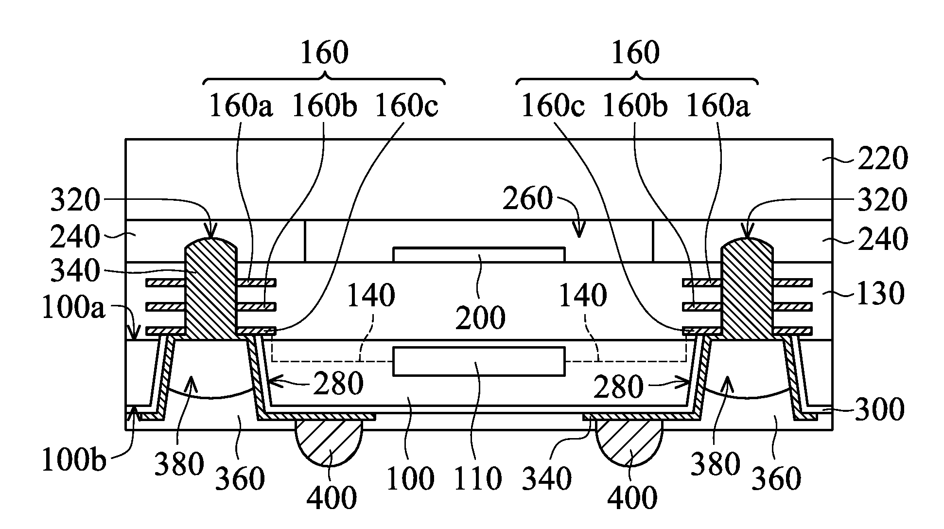
[0015]The making and using of the embodiments of the present disclosure are discussed in detail below. However, it should be noted that the embodiments provide many applicable inventive concepts that can be embodied in a variety of specific methods. The specific embodiments discussed are merely illustrative of specific methods to make and use the embodiments, and do not limit the scope of the disclosure. The disclosed contents of the present disclosure include all the embodiments derived from claims of the present disclosure by those skilled in the art. In addition, the present disclosure may repeat reference numbers and / or letters in the various embodiments. This repetition is for the purpose of simplicity and clarity, and does not imply any relationship between the different embodiments and / or configurations discussed. Furthermore, when a first layer is referred to as being on or overlying a second layer, the first layer may be in direct contact with the second layer, or spaced ap...


PUM


Abstract

A chip package is provided. The chip package includes a substrate having a first surface and a second surface opposite thereto. A dielectric layer is disposed on the first surface of the substrate and includes a conducting pad structure. A first opening penetrates the substrate and exposes a surface of the conducting pad structure. A second opening is communication with the first opening and penetrates the conducting pad structure. A redistribution layer is conformally disposed on a sidewall of the first opening and the surface of the conducting pad structure and is filled into the second opening. A method for forming the chip package is also provided.

Description

CROSS REFERENCE TO RELATED APPLICATIONS[0001]This Application is based on, and claims priority of Taiwan Patent Application No. 103144009, filed on Dec. 17, 2014, the entirety of which is incorporated by reference herein.BACKGROUND OF THE INVENTION[0002]1. Field of the Invention[0003]The invention relates to chip package technology, and in particular to a chip package and methods for forming the same.[0004]2. Description of the Related Art[0005]The chip packaging process is an important step in the fabrication of electronic products. Chip packages not only protect the chips therein from outer environmental contaminants, but they also provide electrical connection paths between the electronic elements inside and those outside of the chip packages.[0006]In conventional chip packages, a conducting layer is in contact with a surface of a signal contact pad so as to form an electrical connection path to those outside of the chip packages.[0007]However, conductance between the signal cont...

Claims


Application Information

Patent Timeline
Patent Type & Authority Applications(United States)
IPC IPC(8): H01L23/00H01L21/78
CPCH01L24/02H01L2224/02317H01L2224/02371H01L21/78H01L21/76802H01L21/76838H01L23/528H01L2224/32013H01L2224/02351H01L2224/024H01L2224/92242H01L2224/0233H01L2924/143H01L2924/141H01L24/05H01L24/11H01L24/13H01L24/29H01L24/32H01L24/73H01L24/83H01L24/92H01L24/94H01L24/95H01L2224/02313H01L2224/02377H01L2224/02381H01L2224/0239H01L2224/0401H01L2224/04026H01L2224/05009H01L2224/05548H01L2224/05611H01L2224/05624H01L2224/05644H01L2224/05647H01L2224/05655H01L2224/05669H01L2224/05687H01L2224/0569H01L2224/1132H01L2224/1146H01L2224/11849H01L2224/13024H01L2224/131H01L2224/13111H01L2224/13116H01L2224/13144H01L2224/13147H01L2224/13155H01L2224/29011H01L2224/29082H01L2224/29186H01L2224/2919H01L2224/32225H01L2224/73253H01L2224/94H01L2224/95H01L2924/1461H01L2224/05572H01L2924/12041H01L23/3114B81B7/0067B81B7/007B81B2201/0292H01L2924/00012H01L2924/01029H01L2924/01079H01L2924/01078H01L2924/01028H01L2924/0105H01L2924/0781H01L2924/0549H01L2924/0543H01L2924/01049H01L2924/0544H01L2924/0542H01L2924/0103H01L2924/00014H01L2924/01013H01L2924/014H01L2224/0231H01L2224/11H01L2224/83H01L2224/81B81C3/00H01L23/315
Inventor LIU, TSANG-YULEE, PO-HANCHIEN, WEI-MING
Owner XINTEC INC
Why Eureka
Try Eureka