
Inspection method for contact by die to database

a technology of contact and database, applied in the direction of image analysis, image enhancement, instruments, etc., can solve the problems of increasing the difficulty of inspection, unable to detect the disconnection due to the small contact, and becoming more difficult to accurately inspect the surface structure of the di

Inactive Publication Date: 2016-04-21
MACRONIX INT CO LTD
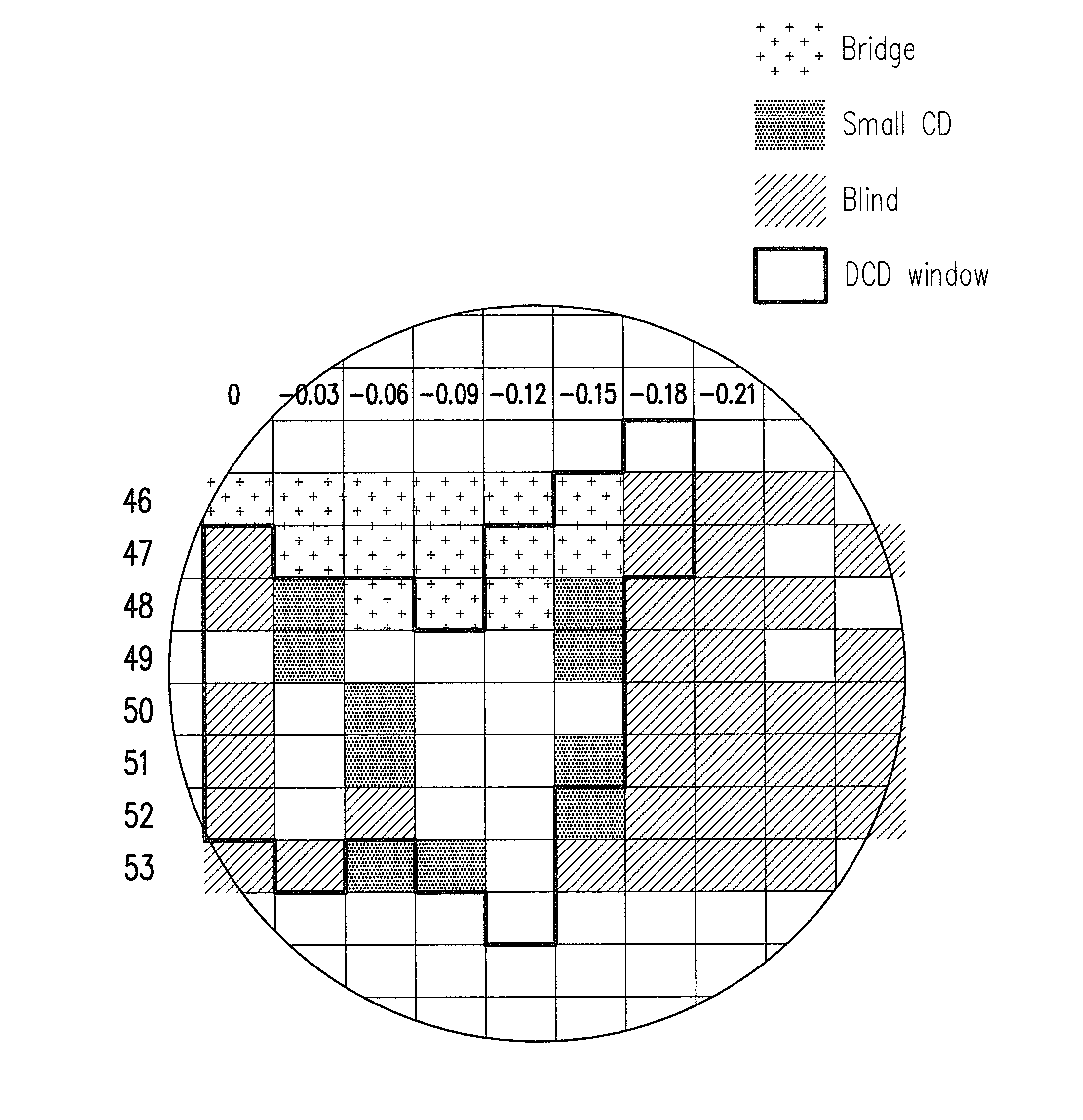
View PDF47 Cites 17 Cited by
  • Summary
  • Abstract
  • Description
  • Claims
  • Application Information

AI Technical Summary

Benefits of technology

The invention provides a method for inspecting contacts on a semiconductor wafer by aligning a machine with a specific position in each die. This ensures accurate inspection of the contacts both in real-time and off-line. Additionally, a "virtual die corner" may be set at the position of each die to improve alignment performance.

Problems solved by technology

In nanometer generation, it becomes more challenging to accurately inspect defects on a surface structure of a die.
However, since the FEM window does not mark a small contact, disconnection due to the small contact may not be detected.
In addition, since the design targets (contact size) in whole chip are different, the difficulty in inspection further increases.
Therefore, it usually takes several months to inspect a die.
Therefore, the E-beam inspection is still insufficient in providing real-time results.

Method used


Image

  • Inspection method for contact by die to database
  • Inspection method for contact by die to database
  • Inspection method for contact by die to database

Examples


Embodiment Construction

[0031]Reference will now be made in detail to the present preferred embodiments of the invention, examples of which are illustrated in the accompanying drawings. Wherever possible, the same reference numbers are used in the drawings and the description to refer to the same or like parts.

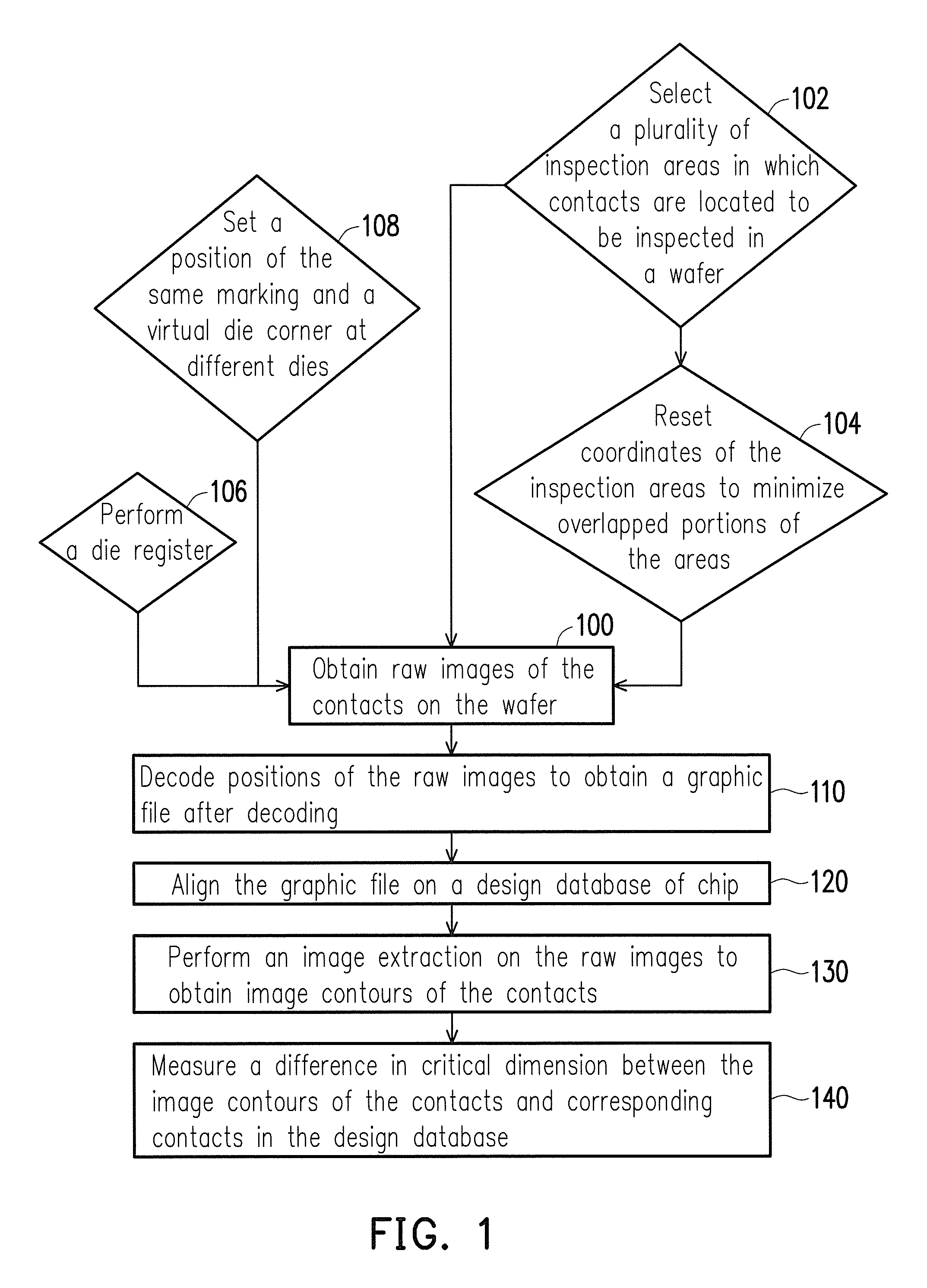
[0032]FIG. 1 is a flowchart illustrating an inspection method for contacts by die to database according to an embodiment of the invention.

[0033]Referring to FIG. 1, at Step 100, raw images of contacts in a wafer are obtained. A method of obtaining the raw image is an E-beam inspection or E-beam SEM review tool (EBR), for example. Although contacts are used as an example to describe this embodiment, the invention is not limited thereto. The method of the invention is generally applicable to parts / positions where the interconnection is desired in a semiconductor device. For example, the image inspection may be utilized on circular apertures or circles such as vias or poly plugs in a wafer or a variety ...


PUM


Abstract

An inspection method for contact by die to database is provided. In the method, a plurality of raw images of contacts in a wafer is obtained, and a plurality of locations of the raw images is then recoded to obtain a graphic file. After that, the graphic file is aligned on a design database of the chip. An image extraction is then performed on the raw images to obtain a plurality of image contours of the contacts. Thereafter, a difference in critical dimension between the image contours of the contacts and corresponding contacts in the design database are measured in order to obtain the inspection result for contacts in the wafer.

Description

BACKGROUND OF THE INVENTION[0001]1. Field of the Invention[0002]The invention relates to a die inspection method, and particularly relates to an inspection method for contacts by die to database (D2DB).[0003]2. Description of Related Art[0004]As line widths continue to shrink in an IC manufacturing process, controlling and monitoring of critical dimensions in the manufacturing process become more and more important. In nanometer generation, it becomes more challenging to accurately inspect defects on a surface structure of a die.[0005]Taking the inspection on contacts for example, there are two common methods. One of the methods is to inspect the contacts after photolithography and etching by using a focus-energy matrix (FEM) of different exposure energies and focuses, so as to define a FEM window. The other is to inspect the contacts by using an E-beam inspection tool.[0006]However, since the FEM window does not mark a small contact, disconnection due to the small contact may not b...

Claims


Application Information

Patent Timeline
IPC IPC(8): G06T7/00
CPCG06T7/0006G06T7/0008G06T2207/30148G06T2207/10061G06T7/001G06T2207/10056G06T7/12
Inventor LUOH, TUUNGLI, HSIAO-LENGYANG, LING-WUUYANG, TA-HONECHEN, KUANG-CHAO
Owner MACRONIX INT CO LTD
Learn More