Imaging device, monitoring device, and electronic device
a monitoring device and imaging device technology, applied in the direction of transistors, color televisions, television systems, etc., can solve the problems of large power consumption of analog/digital, achieve novel structure, reduce power consumption of entire imaging devices, and reduce power consumption. effect of digital processing
- Summary
- Abstract
- Description
- Claims
- Application Information
AI Technical Summary
Benefits of technology
Problems solved by technology
Method used
Image
Examples
embodiment 1
[0067]The configuration of an imaging device in one embodiment of the present invention will be described with reference to FIG. 1.
[0068]In this specification and the like, an imaging device refers to any device having an image capturing function, or alternatively refers to a circuit having an image capturing function or a whole system including the circuit.
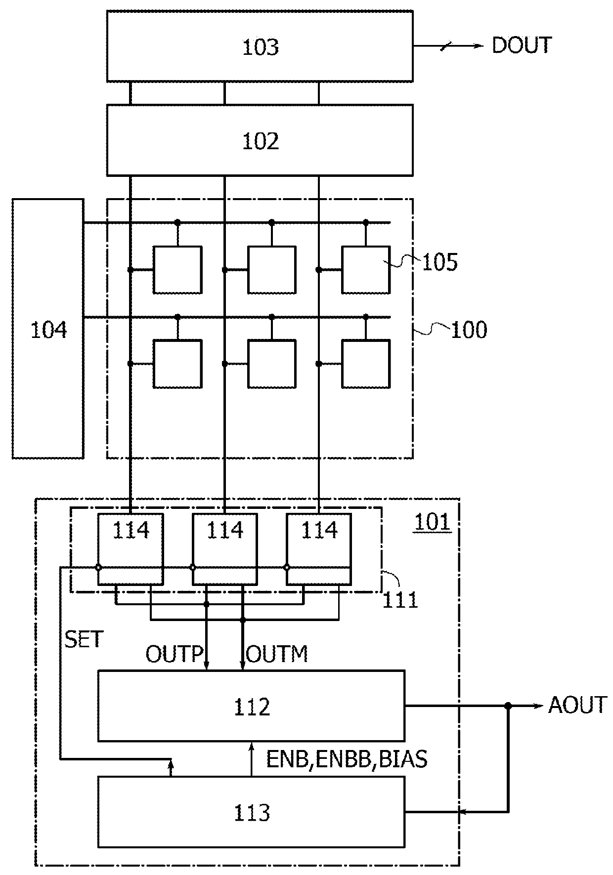
[0069]FIG. 1 is a block diagram illustrating the configuration of the imaging device in one embodiment of the present invention.
[0070]In FIG. 1, an imaging device 10 includes a pixel portion 100, an analog processing circuit 101, an A / D converter circuit 102, a column driver 103, and a row driver 104. The pixel portion 100 includes pixels 105. The analog processing circuit 101 includes a constant current circuit 111, a current comparison circuit 112, and a control circuit 113. The constant current circuit 111 includes constant current sources 114 corresponding to columns of the pixels 105.
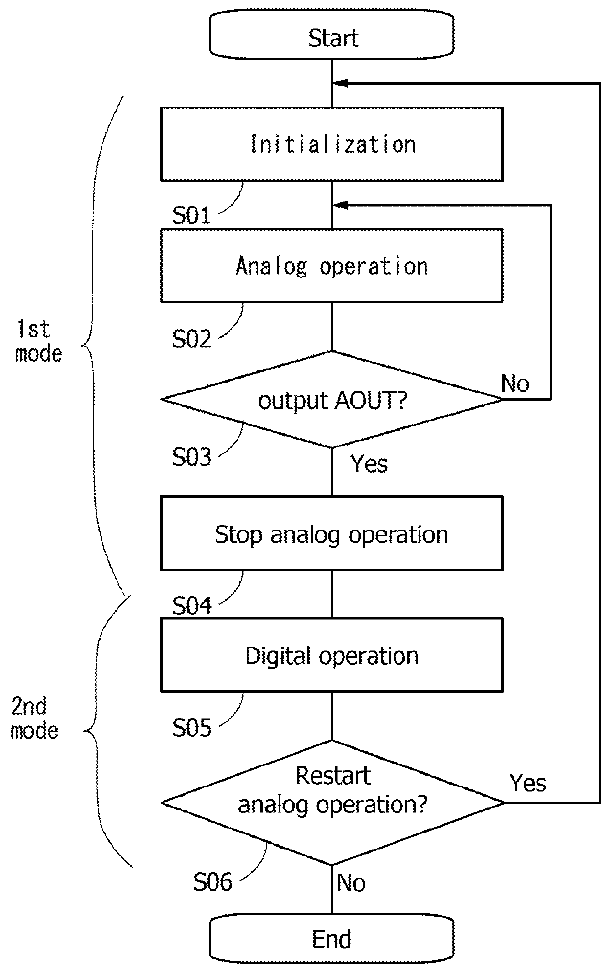
[0071]The imaging device 10 operates in a...
embodiment 2
[0091]This embodiment will explain specific configuration examples of the constant current circuit, the current comparison circuit, and the control circuit included in the analog processing circuit described in Embodiment 1. In this embodiment, the description of the components is based on a configuration that is actually designed; thus, specific numerals used for describing the operation, such as the number of pixels and wirings provided in the row direction and column direction and the frequency of a clock signal and the like, are merely examples.
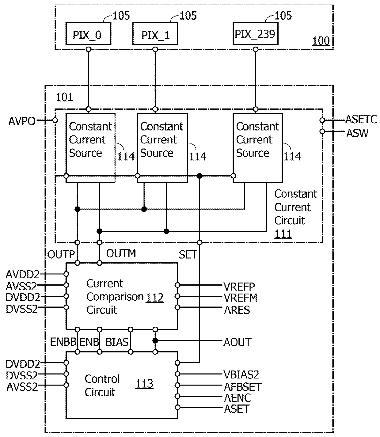
[0092]FIG. 3 is a block diagram illustrating the analog processing circuit 101 and the pixels 105 in the pixel portion 100 electrically connected to the analog processing circuit 101. FIG. 3 illustrates an example where pixels 105 of 240 columns (only first, second, and 240th columns are shown) are provided.
[0093]In the constant current circuit 111, the constant current source 114 is provided for each column. The second current flows betw...
embodiment 3
[0134]In this embodiment, a configuration example of the analog processing circuit that is different from that in Embodiment 2 will be described. Note that the description of the portions described in Embodiment 2 is omitted.
[0135]Like FIG. 3, FIG. 11 is a block diagram illustrating the analog processing circuit 101 and the pixels 105 in the pixel portion 100 electrically connected to the analog processing circuit 101. FIG. 12 illustrates the constant current circuit 111 including a constant current source 310 having a configuration different from that in FIG. 4.
[0136]The configuration of FIG. 11 differs from that of FIG. 3 in that a potential AVREF is supplied instead of the signal ASETC. The configuration of FIG. 12 differs from that of FIG. 4 in that a transistor 313 whose gate is supplied with the potential AVREF is provided instead of the transistors 303 and 304 and the capacitor 307.
[0137]In the constant current circuit 111 of FIG. 11, the potential AVREF is supplied instead o...
PUM
 Abstract
Description
Claims
Application Information
 - R&D
- Intellectual Property
- Life Sciences
- Materials
- Tech Scout
- Unparalleled Data Quality
- Higher Quality Content
- 60% Fewer Hallucinations
Browse by: Latest US Patents, China's latest patents, Technical Efficacy Thesaurus, Application Domain, Technology Topic, Popular Technical Reports.
© 2025 PatSnap. All rights reserved.Legal|Privacy policy|Modern Slavery Act Transparency Statement|Sitemap|About US| Contact US: help@patsnap.com


