
Array substrate and curved display device

Active Publication Date: 2015-12-10
TCL CHINA STAR OPTOELECTRONICS TECH CO LTD
View PDF5 Cites 7 Cited by
  • Summary
  • Abstract
  • Description
  • Claims
  • Application Information

AI Technical Summary

Benefits of technology

The present invention provides a display panel with improved brightness in the area surrounding the edges of the display. This is achieved by a compensation region on the array substrate where dislocation between the array substrate and the color film substrate occurs, resulting in a decreased aperture ratio. The non-compensation region has a normal aperture ratio. During displaying, the main sub pixel charges the data voltage first, while the secondary sub pixel charges the data voltage through a voltage-dividing capacitor, resulting in reduced data voltage in the secondary sub pixel and higher brightness. This ensures that the compensation region displays a higher brightness than the non-compensation region, solving the technical issue of dark area on both sides of the curved display device.

Problems solved by technology

In particular, the black matrix on both sides of the color film substrate would mismatch with the longitudinal data lines on the array substrate.
Some of these data lines would be exposed outside the black matrix and thus block the sub pixel area on the color film substrate, causing a decrease of aperture ratio in this region and further resulting in dark area on both sides of the curved display device.

Method used


Image

  • Array substrate and curved display device
  • Array substrate and curved display device
  • Array substrate and curved display device

Examples


example 1

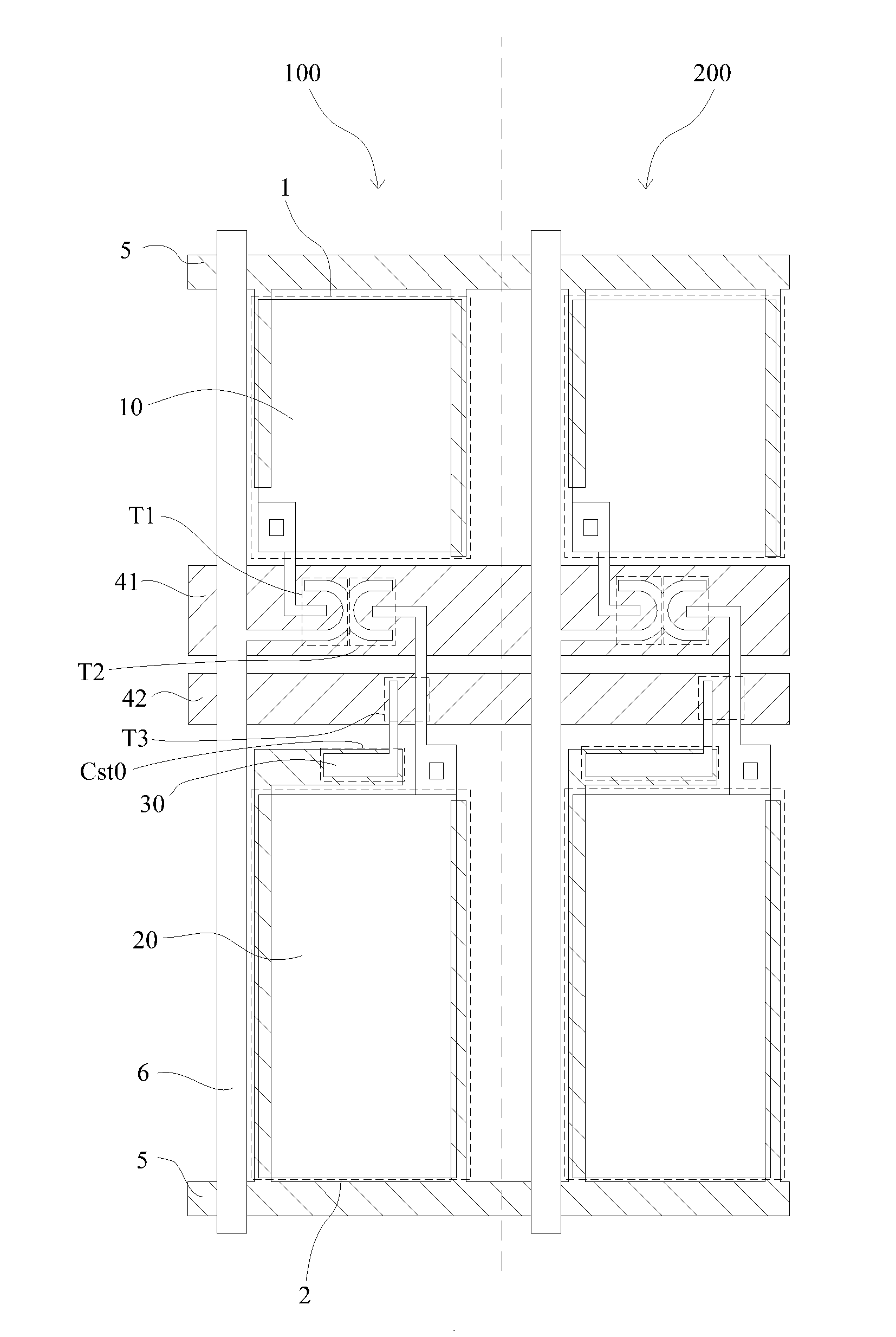
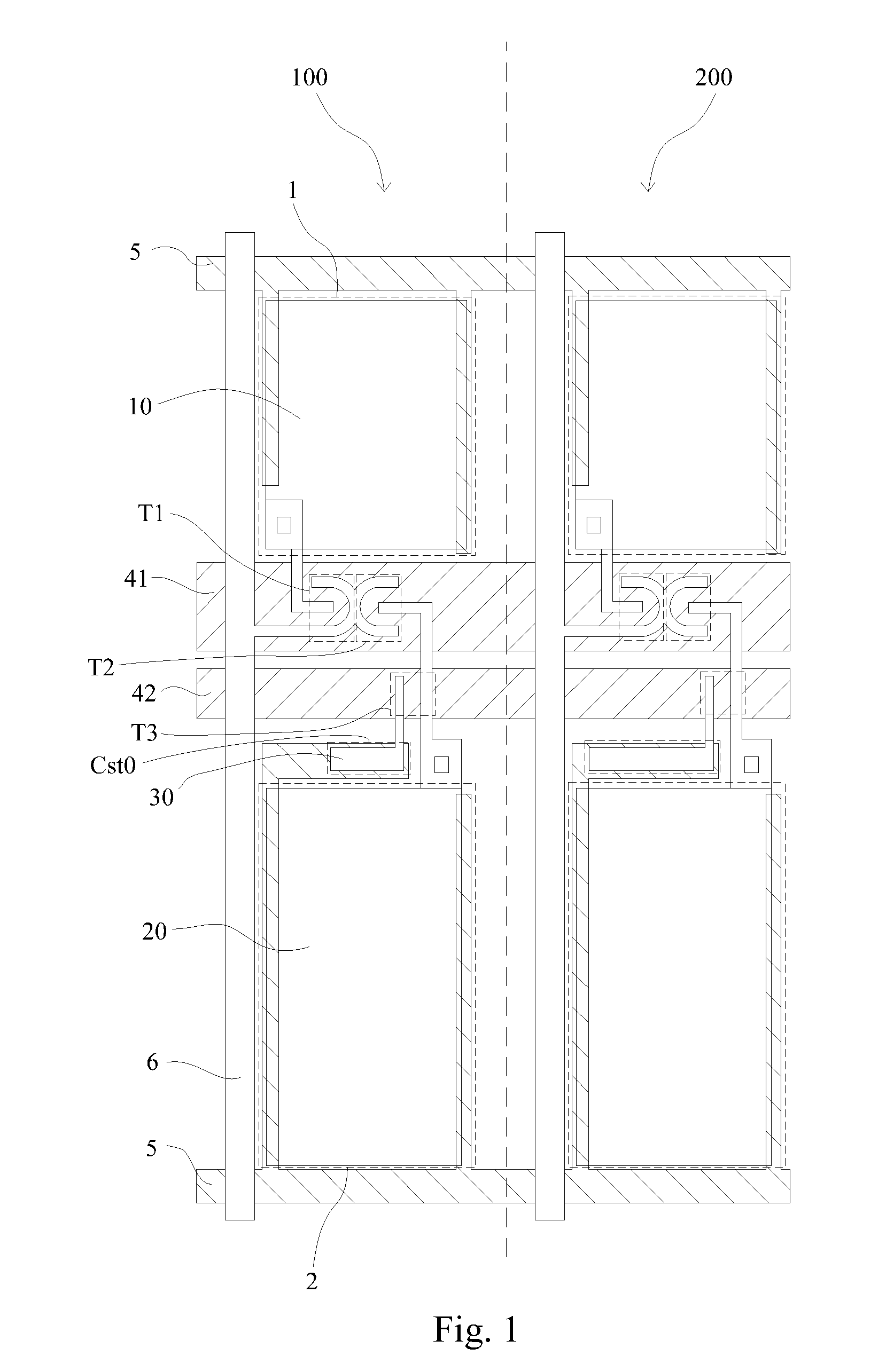
[0033]The array substrate according to Example 1 of the present disclosure comprises a number of sub pixel units arranged as an array. As shown in FIGS. 1 and 2, each sub pixel unit comprises a main sub pixel 1, a secondary sub pixel 2, and a voltage-dividing capacitor (Cst0) 3. The array substrate is divided into a compensation region 100 and a non-compensation region 200. The capacitance of the voltage-dividing capacitor 3 in the compensation region 100 is smaller than that of the voltage-dividing capacitor 3 in the non-compensation region 200.

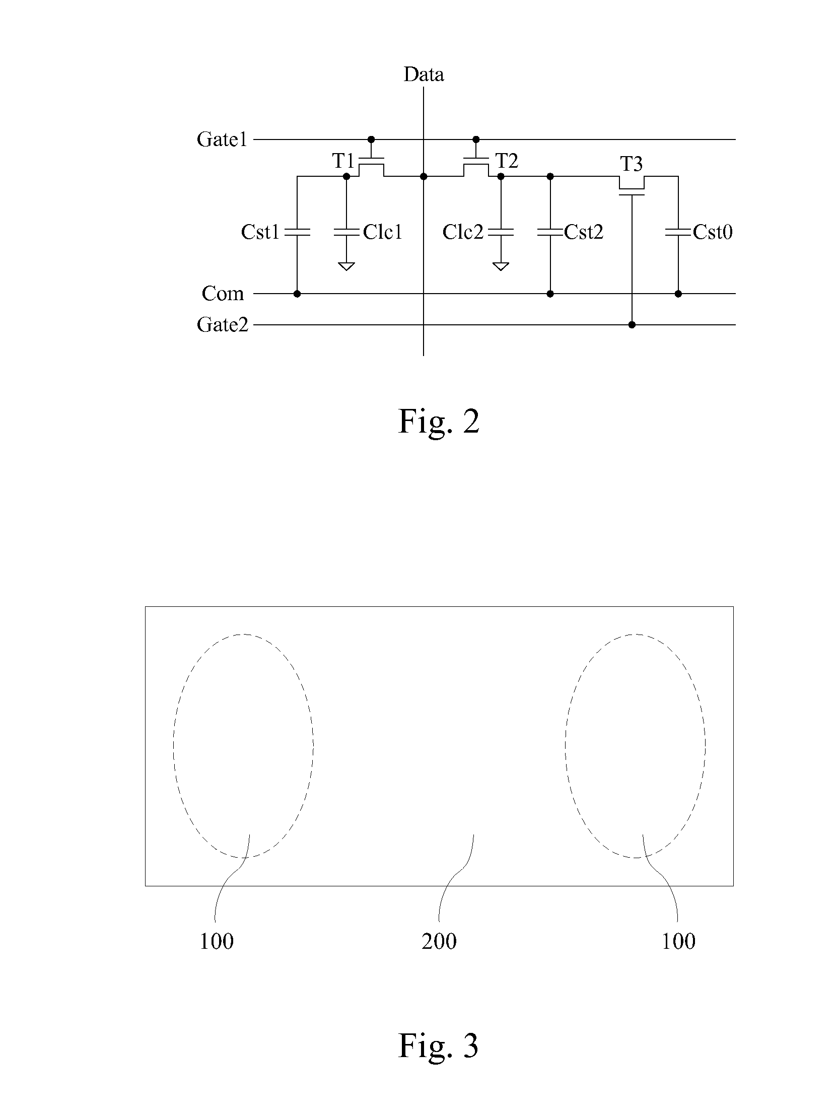
[0034]As shown in FIG. 3, in Example 1, the compensation 100 is the region where dislocation occurs between the array substrate and the color film substrate, i.e. the region having a decreased aperture ratio, and the rest region having a normal aperture ratio is the non-compensation region 200. After the array substrate and the color film substrate are assembled and bent into a curved liquid crystal panel, dislocation between the array subst...

example 2

[0042]The present disclosure further provides a curved display device, which can be a curved television or a curved display, etc. Said curved display device comprises a color film substrate, and an array substrate according to Example 1.

[0043]The curved display device according to Example 2 comprises the same technical features as the array substrate according to Example 1, thus can solve the same technical problem and achieve the same technical effect.

[0044]Preferably, the curved display device is of vertical alignment (VA) type. In a VA type curved display device, by dividing each sub pixel into a main sub pixel and a secondary sub pixel and configuring the liquid crystals in the main sub pixel and the secondary sub pixel with different angles of deflection, the visual angle of the curved display device can be enlarged.

[0045]In Example 2, because the liquid crystal capacitance of the secondary sub pixels in the compensation region is different from that of the secondary sub pixels...


PUM


Abstract

The Present disclosure relates to the field of display technology and discloses an array substrate and a curved display device which can solve the technical problem of dark area on both sides of the existing curved display device. The array substrate according to the present disclosure comprises a number of sub pixel units arranged as an array, each sub pixel unit comprising a main sub pixel, a secondary sub pixel and a voltage-dividing capacitor. Said array substrate is divided into a compensation region and a non-compensation region. The capacitance of the voltage-dividing capacitor of the sub pixel unit in the compensation region is smaller than that of the voltage-dividing capacitor of the sub pixel unit in the non-compensation region. The present disclosure is applicable to curved display devices such as curved television and curved display, etc.

Description

[0001]The present disclosure claims benefit of Chinese patent application CN 201410252392.0, entitled “Array Substrate and Curved Display Device” and filed on Jun. 9, 2014, which is incorporated herein by reference.TECHNICAL FIELD[0002]The present disclosure relates to the technical field of display technology. Specifically, it relates to an array substrate and a curved display device.TECHNICAL BACKGROUND[0003]A curved display device comprises a display screen having a curved shape. Because pixels on the screen of the curved display device each can have the same distance from the human eyes, a true visual perception can be perfectly revivified. Thus, a curved display device is more competitive as compared with a traditional flat panel display device.[0004]The process of manufacturing a curved display device comprises the following steps: separately manufacturing an array substrate and a color film substrate first; then assembling the array substrate and the color film substrate toge...

Claims


Application Information

Patent Timeline
IPC IPC(8): H01L27/12
CPCH01L27/1218H01L27/124H01L27/1255G02F1/136213G02F1/13624G09G3/3659G09G2300/0447G09G2300/0852G09G3/03G02F1/134345G09G3/3648
Inventor GUO, JINBO
Owner TCL CHINA STAR OPTOELECTRONICS TECH CO LTD
Learn More