
Liquid crystal display device

Inactive Publication Date: 2011-05-05
SHARP KK
View PDF6 Cites 2 Cited by
  • Summary
  • Abstract
  • Description
  • Claims
  • Application Information

AI Technical Summary

Benefits of technology

[0026]The present invention provides a liquid crystal display device that can minimize both a decrease in aperture ratio and disturbed alignment of liquid crystal molecules.

Problems solved by technology

In the CPA mode LCD, however, if a pixel region had a low degree of symmetry, the radially tilting alignments of liquid crystal molecules sometimes could not be stabilized.

Method used


Image

  • Liquid crystal display device
  • Liquid crystal display device
  • Liquid crystal display device

Examples


embodiment 1

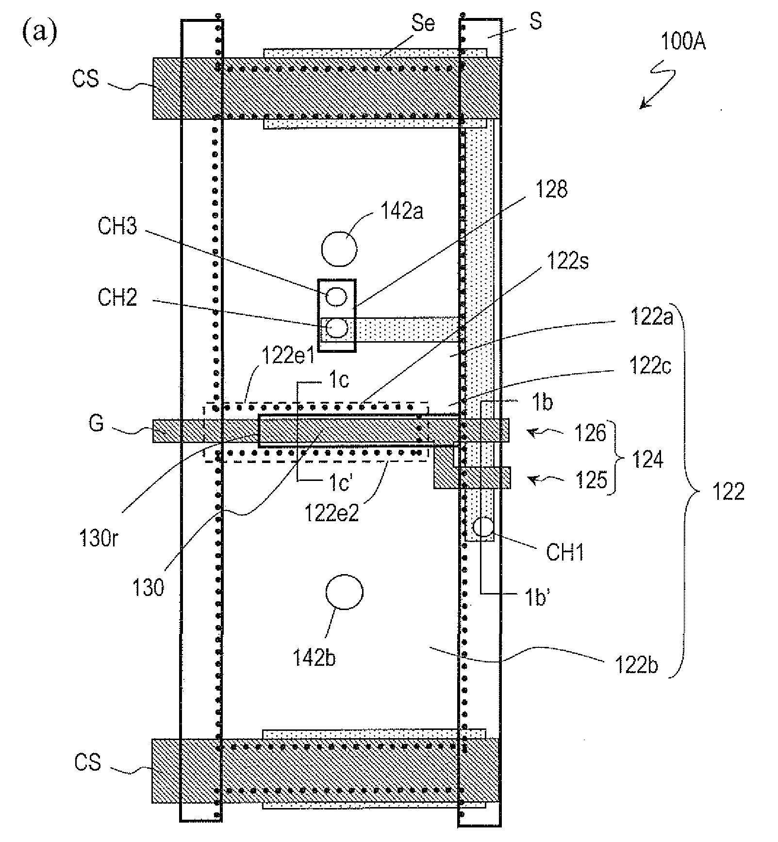
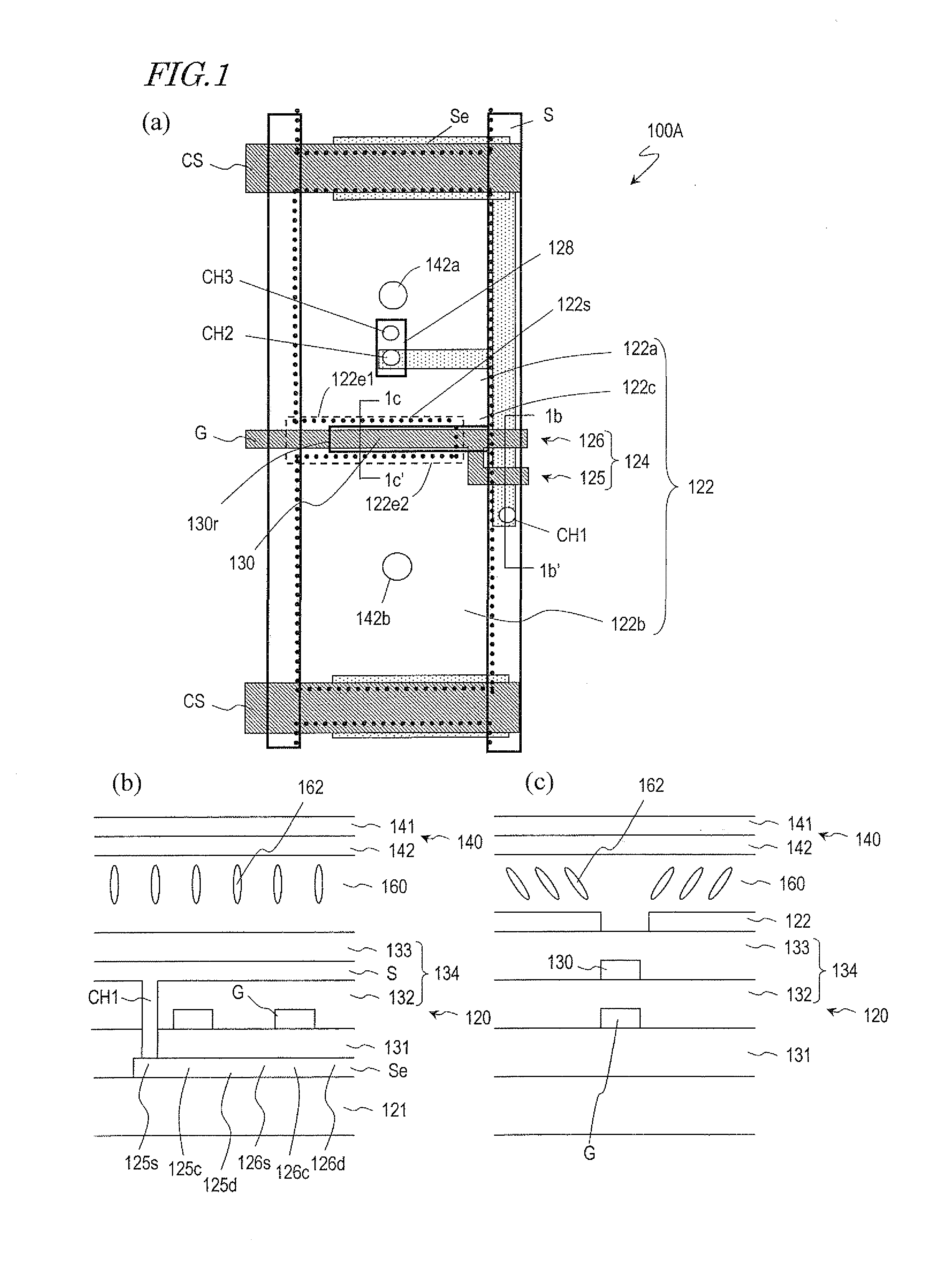
[0037]A first embodiment of a liquid crystal display device according to the present invention will now be described with reference to FIG. 1.

[0038]Specifically, FIG. 1(a) is a schematic plan view illustrating a liquid crystal display device 100A as a first specific embodiment of the present invention, and FIGS. 1(b) and 1(c) are schematic cross-sectional views of the liquid crystal display device 100A as viewed on the respective planes 1b-1b′ and 1c-1c′ shown in FIG. 1(a).

[0039]The liquid crystal display device 100A includes an active-matrix substrate 120, a counter substrate 140 and a liquid crystal layer 160 that is interposed between the active-matrix substrate 120 and the counter substrate 140. The active-matrix substrate 120 includes a transparent substrate 121, gate lines G, source lines S, storage capacitor lines CS, a semiconductor layer Se, pixel electrodes 122, switching elements 124, and drain electrodes 128. The gate lines G run parallel to the storage capacitor lines C...

embodiment 2

[0127]In the above description, the conductive layer 130 is connected to the source line S. However, the present invention is in no way limited to it. The conductive layer 130 could also be connected to the drain electrode 128.

[0128]Hereinafter, a liquid crystal display device 100B as a second embodiment of the present invention will be described with reference to FIG. 8. Specifically, FIG. 8(a) is a schematic representation illustrating the liquid crystal display device 100B, which has the similar configuration as the liquid crystal display device 100A described above except that the conductive layer 130, which is arranged to correspond to the slit 122s of the pixel electrode 122, is connected to the drain electrode 128, instead of the source line S. Thus, the overlapping description will be omitted herein to avoid redundancies.

[0129]In this liquid crystal display device 100B, as viewed along a normal to the principal surface of the active-matrix substrate 120, the conductive layer...


PUM


Abstract

A liquid crystal display device according to the present invention includes: an active-matrix substrate including a pixel electrode, a gate line (G), and a source line (S); a counter substrate including a counter electrode; and a liquid crystal layer. The active-matrix substrate further includes a conductive layer, which is arranged in an insulating layer between the gate line (G) and the pixel electrode. The conductive layer has a portion that is located between the first and second regions of the pixel electrode. And the conductive layer is electrically connected to either the pixel electrode or the source line (S).

Description

TECHNICAL FIELD[0001]The present invention relates to a liquid crystal display device.BACKGROUND ART[0002]Liquid crystal displays (LCDs) have been used in not only TV sets with a big screen but also small display devices such as the monitor screen of a cellphone. TN (twisted nematic) mode LCDs, which would often be used in the past, achieved so narrow viewing angles that LCDs of various other modes with wider viewing angles have been developed one after another. Examples of those wider viewing angle modes include IPS (in-plane switching) mode and VA (vertical alignment) mode. Among those wide viewing angle modes, the VA mode is adopted in a lot of LCDs because the VA mode would achieve a sufficiently high contrast ratio.[0003]Known as a kind of VA mode LCD is an MVA (multi-domain vertical alignment) mode LCD in which multiple liquid crystal domains are defined within a single pixel region (see Patent Documents Nos. 1 and 2, for example). In an MVA mode LCD, an alignment regulating s...

Claims


Application Information

Patent Timeline
IPC IPC(8): G02F1/1343
CPCG02F1/136286G02F1/133707
Inventor KATSUMOTO, KAZUNARITASAKA, YASUTOSHI
Owner SHARP KK
Learn More