
Techniques for Generating Nanowire Pad Data from Pre-Existing Design Data

Inactive Publication Date: 2015-12-10
IBM CORP
View PDF5 Cites 6 Cited by
  • Summary
  • Abstract
  • Description
  • Claims
  • Application Information

AI Technical Summary

Benefits of technology

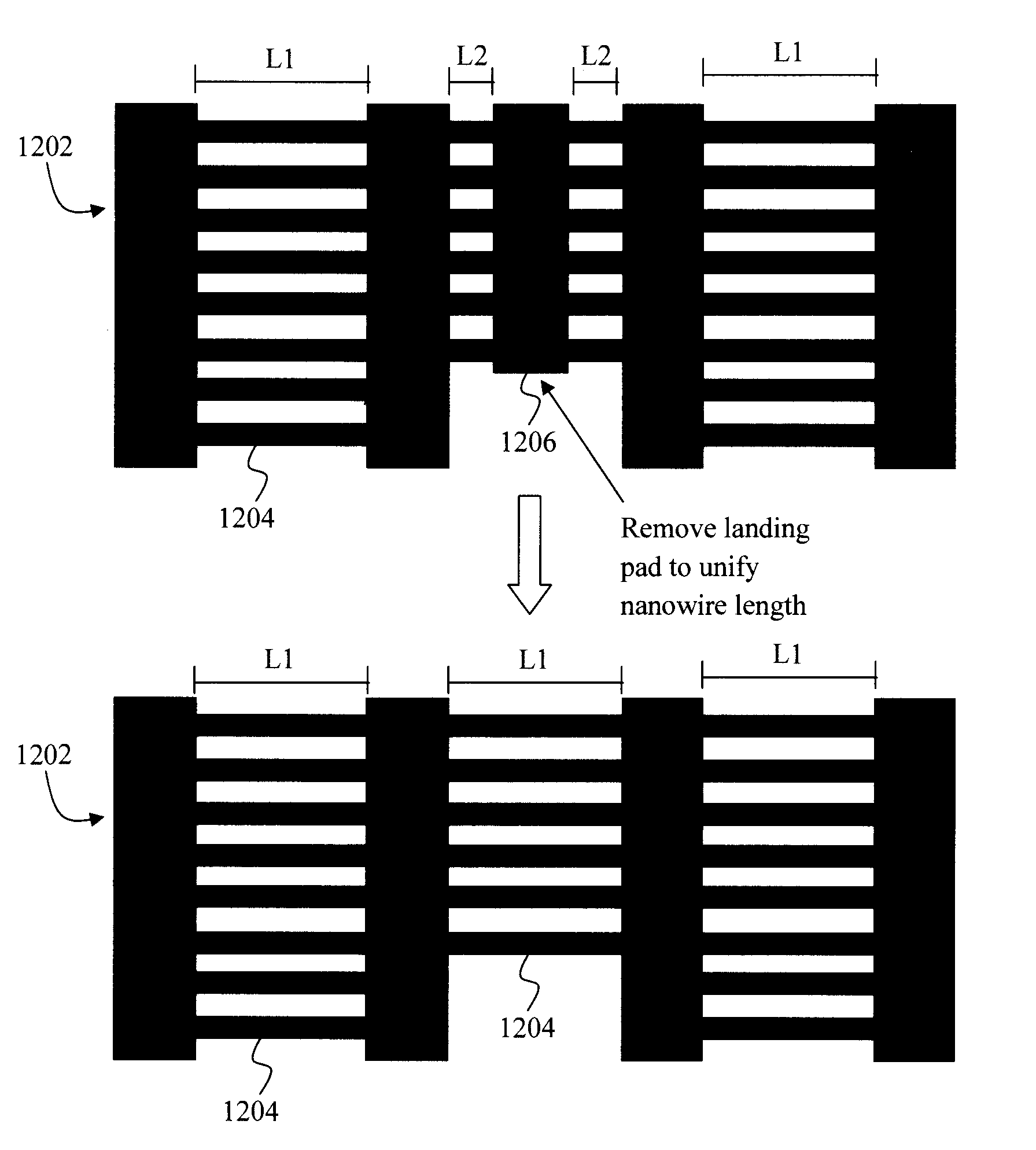
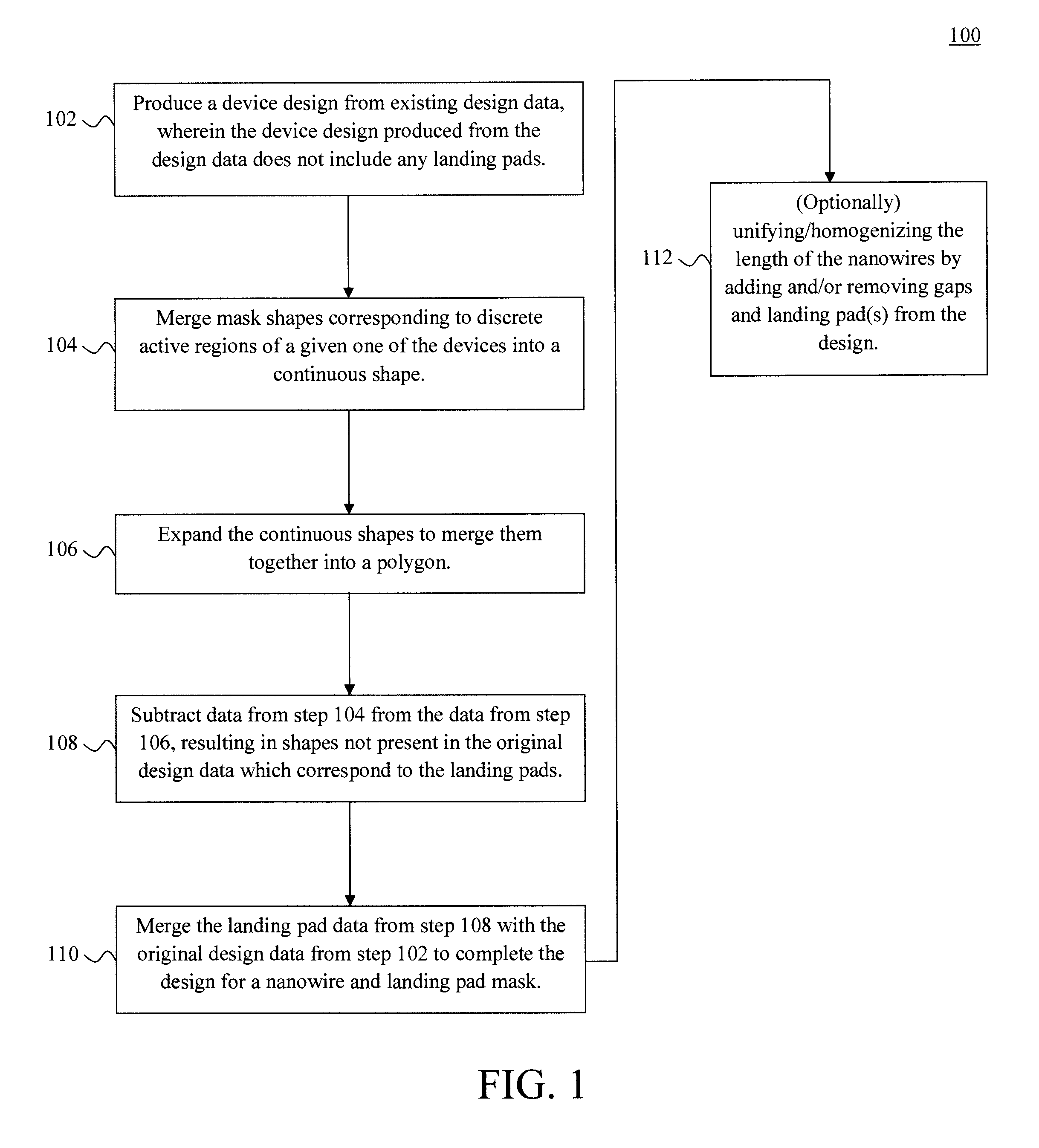
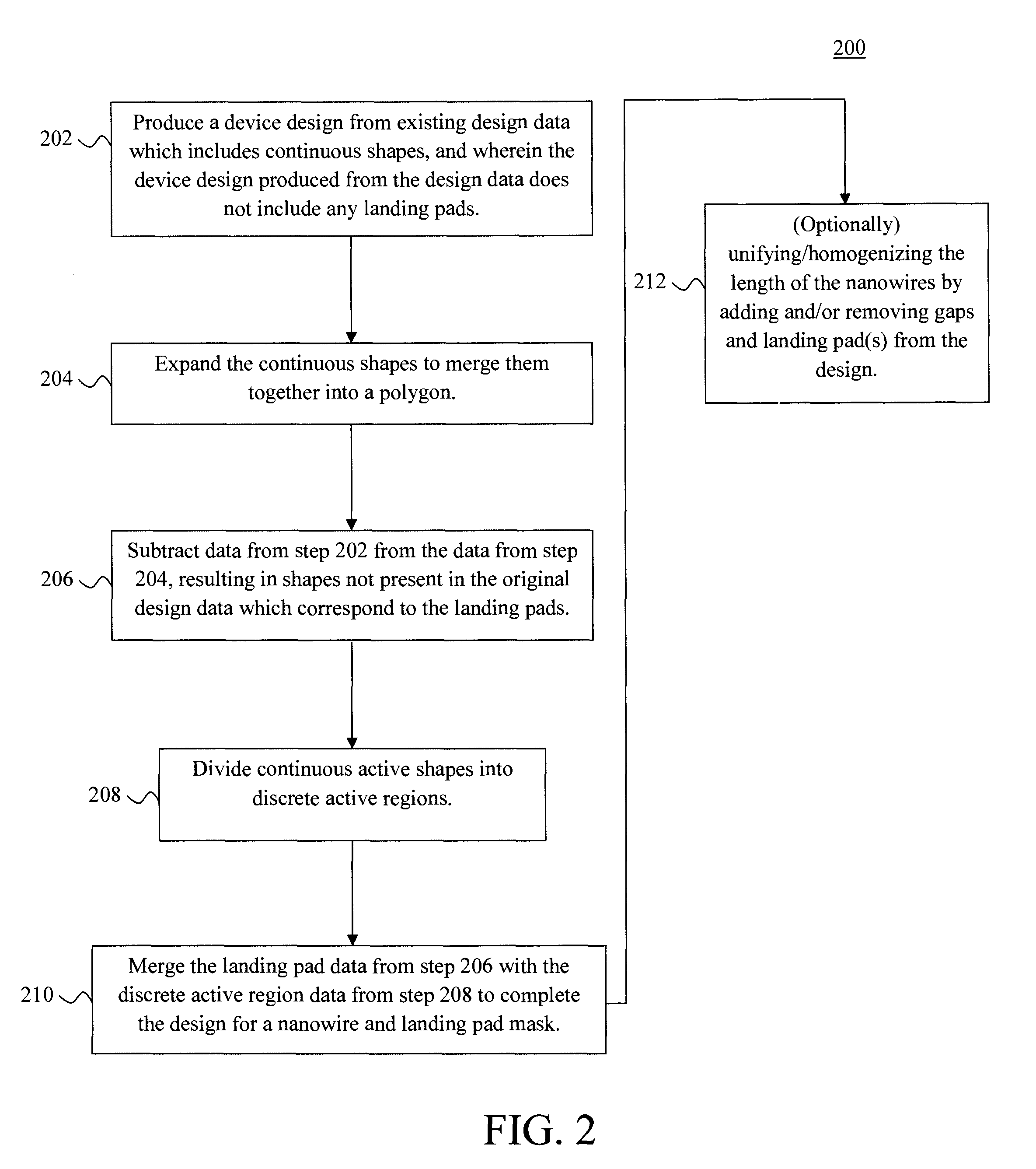
The present invention provides techniques for automatically adding nanowire landing pads to existing device designs, such as FIN field effect transistor or planar complementary metal oxide semiconductor designs. A computer-aided design method is used to create a lithographic mask which includes the nanowire mask shapes and the landing pad shapes for anchoring the nanowire mask shapes. This invention enables the efficient and automated creation of lithographic masks for nanowire-based devices.

Problems solved by technology

However, the specifications of the various devices in the design oftentimes vary from one device to another.
Based on this device variation, manually placing each of the landing pads in the correct location in the design can be an extremely time-consuming process.

Method used


Image

  • Techniques for Generating Nanowire Pad Data from Pre-Existing Design Data
  • Techniques for Generating Nanowire Pad Data from Pre-Existing Design Data
  • Techniques for Generating Nanowire Pad Data from Pre-Existing Design Data

Examples


Embodiment Construction

[0024]As highlighted above, electronic device designs employing freely suspended wires also need landing pads to tether or anchor the wires. One implementation of a nanowire / landing pad design employs a ladder-like configuration wherein both the nanowires and pads are patterned in an active layer of a wafer wherein the nanowires, like the rungs of a ladder, have the pads attached at opposite ends thereof. See, for example, FIG. 8 (described below) which depicts such a ladder-like nanowire and pad configuration.

[0025]In implementations involving silicon-on-insulator (SOI) wafers, an SOI layer is the active layer in which the nanowires and pads are patterned. In an SOI wafer, the SOI layer is typically separated from a supporting substrate by a buried oxide (or BOX). To form the device, a hardmask is patterned on the SOI layer with the footprint and location of the nanowires and landing pads. The shape of the patterned hardmask is then transferred to the SOI layer (e.g., using a suita...


PUM


Abstract

In one aspect, a CAD-based method for designing a lithographic mask for nanowire-based devices is provided which includes the steps of: create a design for the mask from existing (e.g., FINFET or planar CMOS) design data which includes, for each of the devices, one or more nanowire mask shapes (FINFET design data) or continuous shapes (planar CMOS design data); for FINFET design data, merging the nanowire mask shapes into continuous shapes; expanding the continuous shapes to join all of the continuous shapes in the design together forming a single polygon shape; removing the continuous shapes from the single polygon shape resulting in landing pad shapes for anchoring the nanowire mask shapes; for CMOS design data, dividing the continuous active shapes into one or more nanowire mask shapes; and merging the landing pad shapes with the nanowire mask shapes to form the lithographic mask.

Description

FIELD OF THE INVENTION[0001]The present invention relates to nanowire-based devices having landing pads to anchor / tether the nanowires, and more particularly, to techniques for automatically placing nanowire landing pads in a device design derived from existing design data (e.g., FIN field effect transistor (FINFET) or planar complementary metal oxide semiconductor (CMOS) design data) which does not already include landing pads in the design.BACKGROUND OF THE INVENTION[0002]Gate-all-around (or GAA) nanowire devices are a promising candidate for complementary metal oxide semiconductor (CMOS) device scaling. Some GAA nanowire device designs form the gate electrode around a freely suspended wire(s). In that case, each freely suspended wire requires tethering, anchor or landing pad structures.[0003]For silicon-on-insulator (SOI) nanowires this can be formed by making a landing pad of continuous SOI adjacent to a grouping of nanowires. Thus, multiple nanowires can share the same landing ...

Claims


Application Information

Patent Timeline
IPC IPC(8): G06F17/50H01L29/78
CPCH01L29/785G06F17/5068H01L21/84G06F30/392G06F30/39H01L29/0669G06F2119/18G03F1/70G06F2111/14
Inventor BALAKRISHNAN, KARTHIKCHANG, JOSEPHINE B.GUILLORN, MICHAEL A.SLEIGHT, JEFFREY W.
Owner IBM CORP
Learn More