Liquid crystal display device
a liquid crystal display and display device technology, applied in non-linear optics, instruments, optics, etc., can solve the problems of comparatively weak bond strength between organic film and inorganic film, the problem of bonding force and the problem of bonding between the alignment film and the underlying film thereo
- Summary
- Abstract
- Description
- Claims
- Application Information
AI Technical Summary
Benefits of technology
Problems solved by technology
Method used
Image
Examples
first embodiment
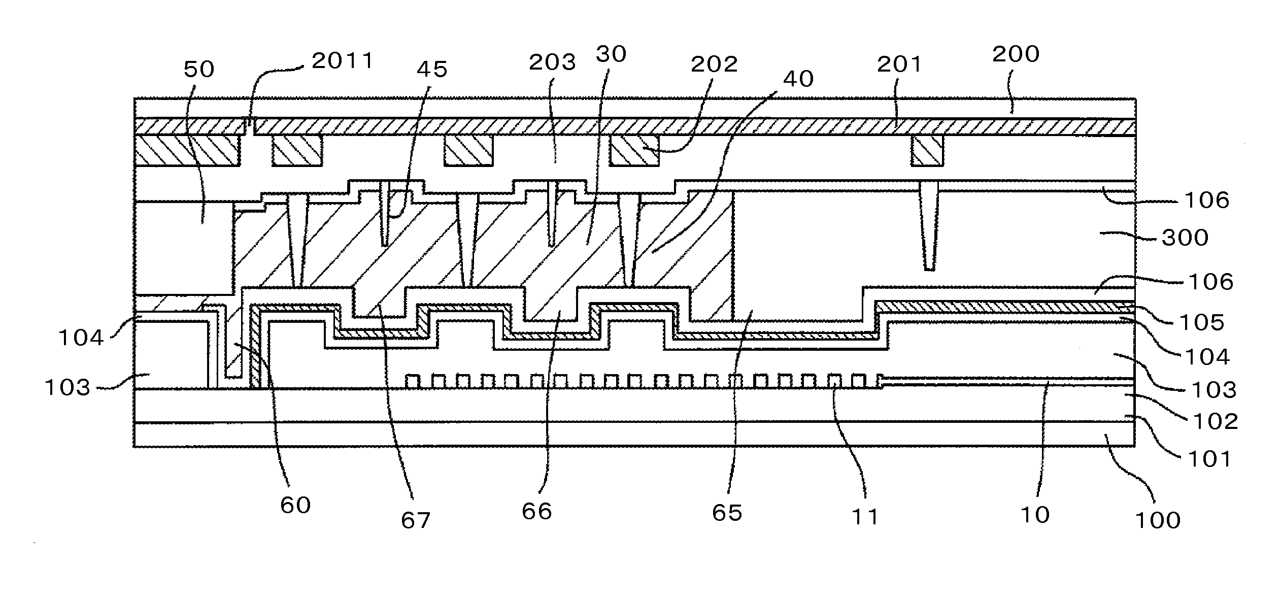
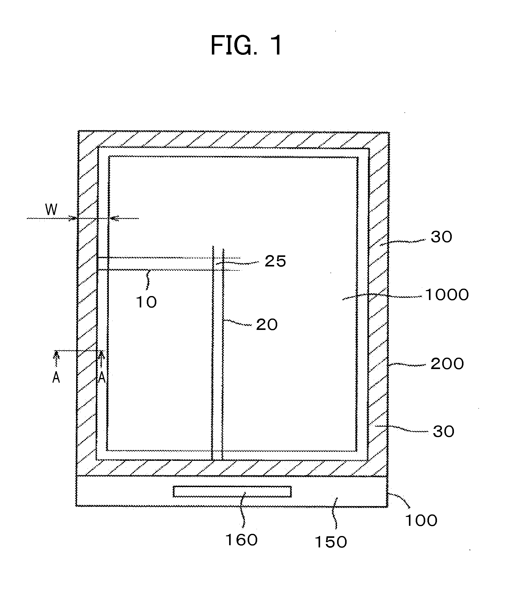
[0049]FIG. 1 is a plan view showing a liquid crystal display device to which the present invention is applied. Referring to FIG. 1, the TFT substrate 100 and the counter substrate 200 are bonded together by the sealing material 30 while the liquid crystal is sandwiched between the TFT substrate 100 and the counter substrate 200. The TFT substrate 100 is formed in a larger size than the counter substrate 200. A portion of the TFT substrate 100 that extends as a single layer defines a terminal part 150. The terminal part 150 is formed with an IC driver 160 for driving a liquid crystal display panel, terminals for connection of a flexible wiring board for supplying electric power, image signals, scan signals and the like to the liquid crystal display panel, and the like.
[0050]Referring to FIG. 1, a display region 1000 includes scanning lines 10 extended horizontally and arranged vertically, and further includes image signal lines 20 extended vertically and arranged horizontally. An are...
second embodiment
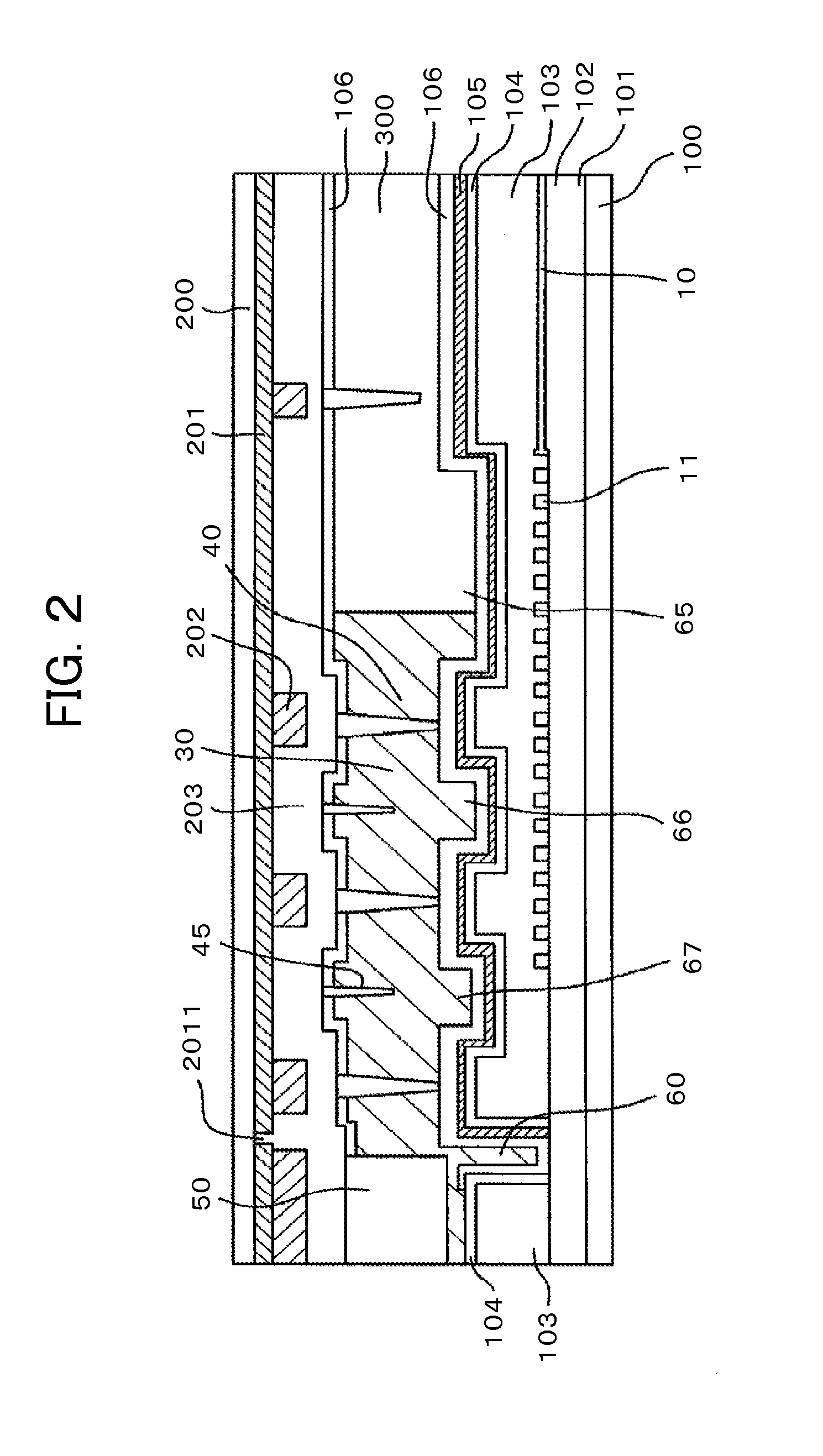
[0071]FIG. 7 is a sectional view showing as second embodiment of the present invention. FIG. 7 is a sectional view also corresponding to the sectional view taken on the line A-A in FIG. 1. FIG. 7 differs from FIG. 2 of the first embodiment in that the ITO 105 formed on the TFT-substrate 100 side does not extend so far as an inside edge of the sealing material 30. In this case, as well, the ITO 105 exists between the alignment film 106 and the interlayer insulating film 104 at a main portion of the sealing material 30 and hence, the separation of the alignment film 106 at the seal part 30 can be prevented. The other components in FIG. 7 are the same as those of FIG. 2.
[0072]FIG. 8 is a plan view of the TFT substrate 100 corresponding to the structure of FIG. 7, or a schematic diagram showing relationships among the display region 1000, the range of the ITO 105, the interlayer insulating film 104, the groove-like through-hole 60 and the like. Referring to FIG. 8, an area outside the d...
PUM
| Property | Measurement | Unit |
|---|---|---|
| transparent | aaaaa | aaaaa |
| distance | aaaaa | aaaaa |
| thickness | aaaaa | aaaaa |
Abstract
Description
Claims
Application Information
 - R&D
- Intellectual Property
- Life Sciences
- Materials
- Tech Scout
- Unparalleled Data Quality
- Higher Quality Content
- 60% Fewer Hallucinations
Browse by: Latest US Patents, China's latest patents, Technical Efficacy Thesaurus, Application Domain, Technology Topic, Popular Technical Reports.
© 2025 PatSnap. All rights reserved.Legal|Privacy policy|Modern Slavery Act Transparency Statement|Sitemap|About US| Contact US: help@patsnap.com


