
Gate driving circuit, gate driving method and display device

Active Publication Date: 2015-11-12
BOE TECH GRP CO LTD +1
View PDF2 Cites 33 Cited by
  • Summary
  • Abstract
  • Description
  • Claims
  • Application Information

AI Technical Summary

Benefits of technology

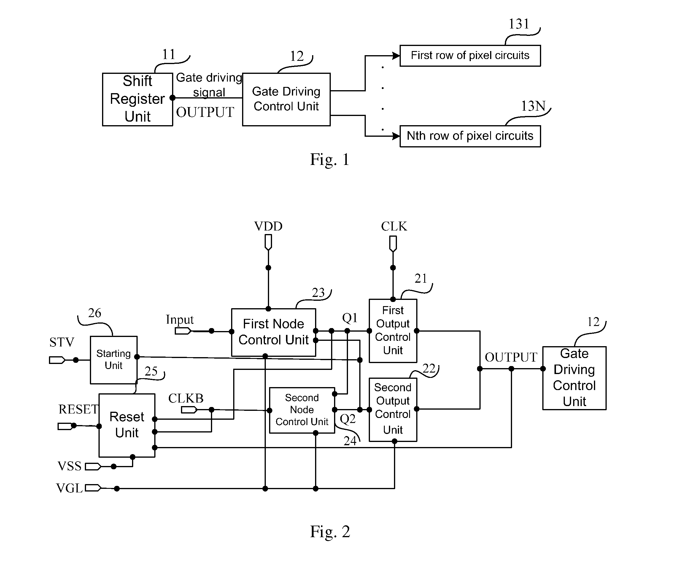
This patent describes a new way to design a circuit for driving pixels in a display device. Rather than using just one shift register unit to drive one row of pixels, this new design uses multiple cascaded shift register units. This saves space and allows the display device to have a narrower bezel, even if it has a high pixel per inch (PPI) resolution.

Problems solved by technology

How to realize the narrow bezel of liquid crystal display panels of high PPI adopting a-Si technology is a problem currently to be solved urgently.

Method used


Image

  • Gate driving circuit, gate driving method and display device
  • Gate driving circuit, gate driving method and display device
  • Gate driving circuit, gate driving method and display device

Examples


Embodiment Construction

[0068]The technical solutions in the embodiments of the present disclosure will be described clearly and thoroughly with reference to the drawings of the embodiments of the present disclosure. Obviously, the embodiments described are only part of, rather than all of, the embodiments of the present disclosure. All other embodiments conceived by a person skilled in the art based on the embodiments of the present disclosure without doing any creative work shall fall within the protection scope of the present disclosure.

[0069]All of the transistors adopted in all embodiments of the present disclosure can be thin film transistors or field effect transistors or other devices that having the same property. In the embodiments of the present disclosure, in order to distinguish the two electrodes other than the gate electrode in the transistor, one electrode is called as a source electrode, and the other one is called as a drain electrode. In addition, transistors can be divided into N type t...


PUM


Abstract

The present disclosure discloses a gate driving circuit, a gate driving method and a display device. The gate driving circuit includes a plurality of cascaded shift register units for outputting gate driving signals, each of the gate driving signals being output by a gate driving signal output terminal of each shift register unit; the gate driving circuit further includes: a gate driving control unit connected with the shift register unit for controlling the gate driving signal to be transmitted to N rows of pixel circuits time-divisionally, wherein N is a positive integer greater than or equal to 2.

Description

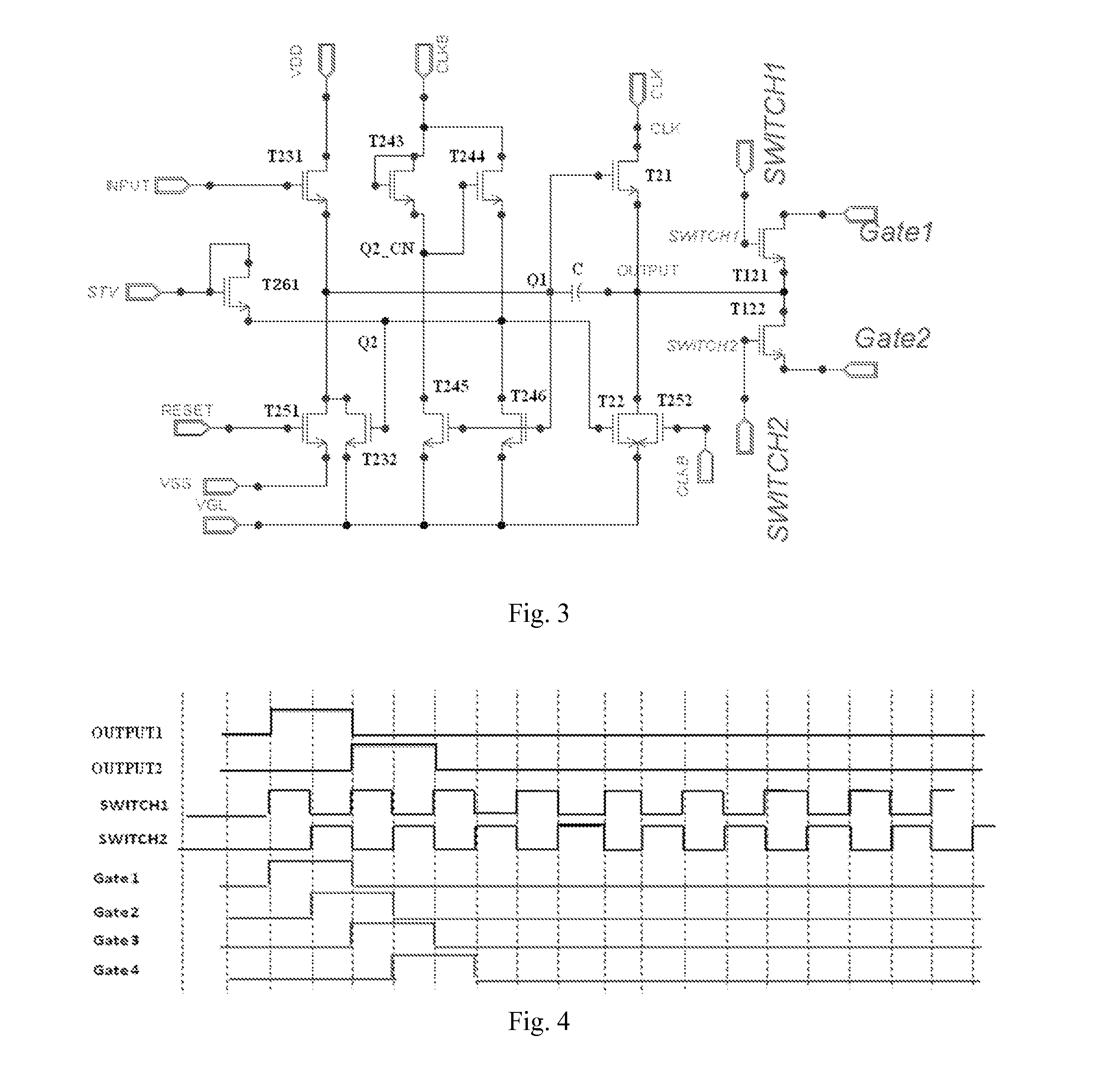
CROSS-REFERENCE TO RELATED APPLICATION[0001]The present disclosure claims the priority right of Chinese patent application No. 201410193283.6 filed on May 8, 2014, the whole content of which is incorporated herein for reference.TECHNICAL FIELD[0002]The present disclosure relates to the display technology field, and in particular, to a gate driving circuit, a gate driving method and a display device.BACKGROUND[0003]As the resolution of a liquid crystal display panel is becoming higher and higher, PPI (Pixels per inch) also gets higher and higher. Narrow bezel is required for a liquid crystal display panel of high PPI, therefore, all current liquid crystal display panels of high PPI adopt the LTPS (Low Temperature Poly-silicon) technology. How to realize the narrow bezel of liquid crystal display panels of high PPI adopting a-Si technology is a problem currently to be solved urgently.SUMMARY[0004]The main purpose of the present disclosure is to provide a gate driving circuit, a gate d...

Claims


Application Information

Patent Timeline
IPC IPC(8): G09G3/36G11C19/28
CPCG09G3/36G11C19/28G09G2310/0205G09G2300/0465G09G2310/0286G09G3/3677
Inventor WANG, SHIJUN
Owner BOE TECH GRP CO LTD
Learn More