
Method and System for Near Field Communication of Electronic Device

a technology of electronic devices and methods, applied in the field of near field communication, can solve the problems of substantially inability to communicate and inability to ensure communication quality, and achieve the effect of ensuring communication quality

Active Publication Date: 2015-10-01
SHENZHEN GOODIX TECH CO LTD
View PDF28 Cites 8 Cited by
  • Summary
  • Abstract
  • Description
  • Claims
  • Application Information

AI Technical Summary

Benefits of technology

The present invention is a method and system for near field communication that solves the problem of interference between different electronic devices. It detects interference frequencies and selects frequency points with smaller interference for data transmission. This ensures that interference frequency points are shielded from data transmission, improving communication quality.

Problems solved by technology

However, as a detectable signal of near field communication is comparatively weak and easily suffers from electromagnetic interference in a communication environment, communication quality cannot be ensured.
For example, in an application situation of touch screen, when the communication between two devices is not established, because the communication signal between the two touch screens is very weak; meanwhile, the capacitive screens are generally very close to an LCD, the driving signal of the LCD would disturb the communication signal between the capacitive screens, and in a case that the display screen is switched on, the communication is substantially unable if the interference is received.

Method used


Image

  • Method and System for Near Field Communication of Electronic Device
  • Method and System for Near Field Communication of Electronic Device
  • Method and System for Near Field Communication of Electronic Device

Examples


embodiment 1

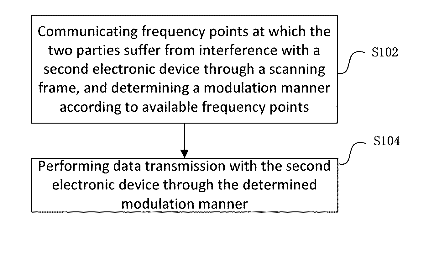
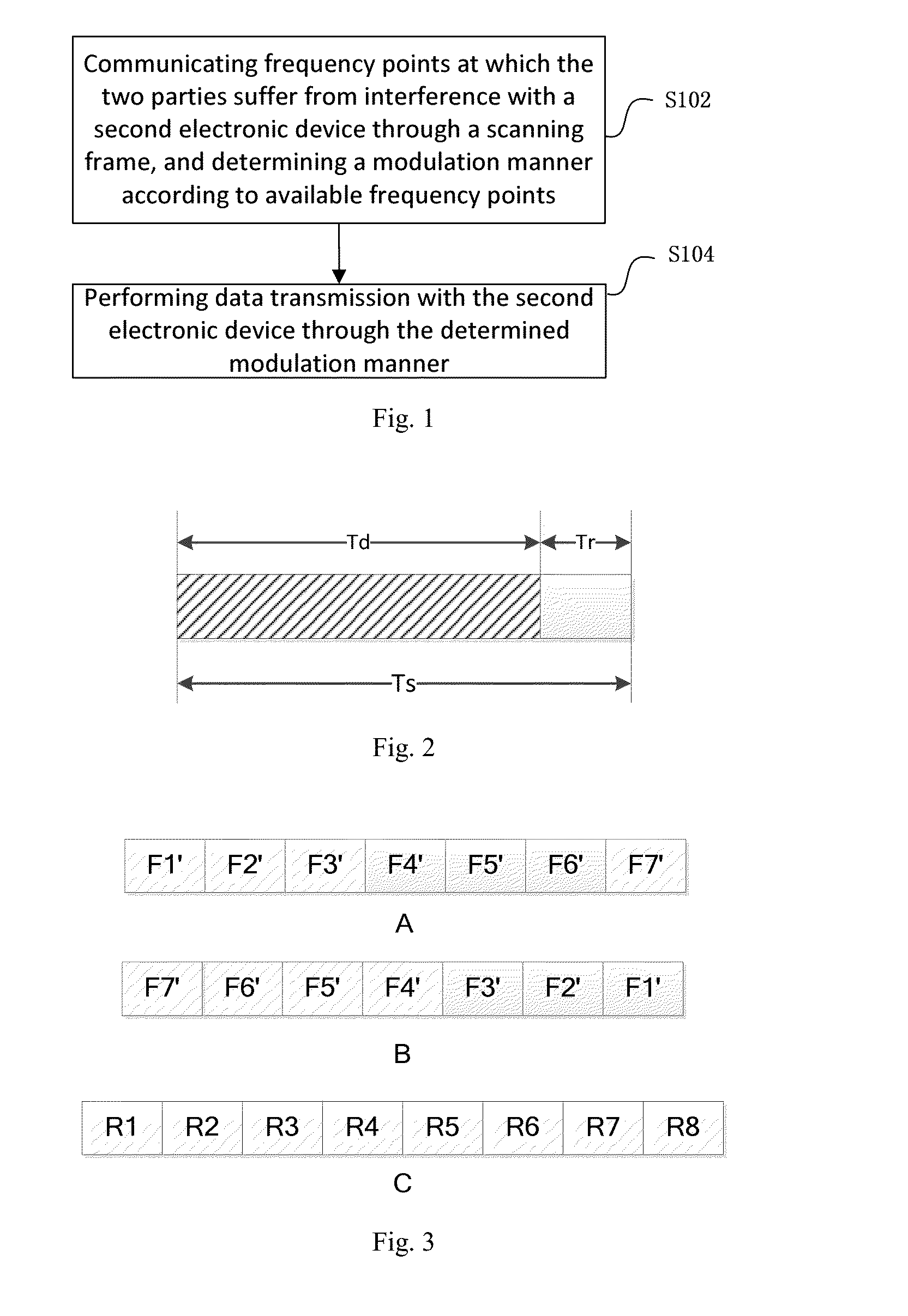
[0063]FIG. 1 shows a flow chart of a method for near field communication of an electronic device provided by the embodiment of present invention, wherein the method is applied to a Master, and when the Master does not detect a second electronic device, a touch detection and an approach detection may be multiplexed, and when the second electronic device within a nearby communicable range is detected, the touch detection is paused and the near field communication is started. It specifically comprises the following steps:

[0064]S102, communicating frequency points at which the two parties suffer from interference with a Slave through a scanning frame, and determining a modulation manner according to available frequency points, wherein the scanning frame comprises at least two symbols modulated by using different frequencies.

[0065]Please refer to FIG. 2, symbol is the minimum communication unit for carrying bit data, and a modulation manner of the symbol employs a manner similar to FSK (...

embodiment 2

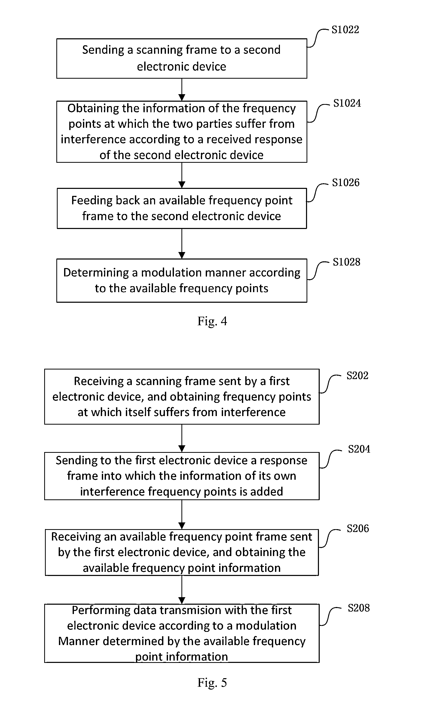
[0074]FIG. 4 is a flow chart of a method for frequency scanning provided by the preferred embodiment of the present invention, wherein the method is applied to a Master. Refer to the FIG. 3 for the construction of a frame structure, and the method comprises the following steps:

[0075]S1022, the Master sending a scanning frame A to a Slave;

[0076]S1024, obtaining frequency points at which the two parties suffer from interference according to a received response of the Slave;

[0077]In detail, obtaining information of the frequency points at which the two parties suffer from interference according to a received response frame C1 responded by the Slave; or obtaining its own interference frequency point information through the scanning frame responded by the Slave, and obtaining the information of the frequency points at which the Slave suffers from interference according to the response frame responded by the Slave, wherein, the Master determines the interference frequency point informatio...

embodiment 3

[0090]FIG. 5 shows a flow chart of another method for frequency scanning provided by the preferred embodiment of the present invention, wherein the method is applied to a Slave and specifically comprises the following steps:

[0091]S202, receiving a scanning frame A sent by a Master, and obtaining its own frequency points that suffer from interference.

[0092]S204, feeding back to the Master a response frame in which its own interference frequency point information is added.

[0093]In detail, the response frame may be obtained in the following manner:

[0094]When there is no interference frequency point, the response frame is obtained by, after the scanning frame is inverted, appending any one of frequency point symbols in the scanning frames at the end;

[0095]When there is only one interference frequency point, the response frame is obtained by moving the interference frequency point to be after the scanning frame, and moving forwards frequency point symbols after the interference frequency...


PUM


Abstract

A method and a system for near field communication of an electronic device are disclosed. The method comprises: communicating frequency points at which the two parties suffer from interference with a second electronic device through a scanning frame, wherein the scanning frame comprises at least two symbols modulated by using different frequencies; and determining a modulation manner according to the available frequency points in order to perform data transmission with the second electronic device. With the embodiment of the present invention, interference frequencies in the communication environment are detected by sending the scanning frame which comprises at least two symbols modulated by using different frequencies, and frequency points with smaller interference are selected for adaptation modulation data, thus the interference frequency points are shielded from data transmission, and external interference in the near field communication is avoid, and communication stability is improved, and communication quality is improved.

Description

TECHNICAL FIELD[0001]The present invention belongs to a technical field of near field communication, and particularly relates to a method and a system for near field communication of an electronic device.BACKGROUND ART[0002]Non-contact point-to-point data transmission is enabled within about ten centimeters between electronic devices through Near Field Communication (NFC) utilizing electric field. Due to its low transmission power, near communication distance, and comparatively high security, the NFC is widely applied in the industry of logistics, payment, finance and warehouse management, etc. As the rise of wireless internet and common usage of smart-phone, the usage of functions of mobile payment, material sharing and the like becomes more and more widely.[0003]However, as a detectable signal of near field communication is comparatively weak and easily suffers from electromagnetic interference in a communication environment, communication quality cannot be ensured. For example, i...

Claims


Application Information

Patent Timeline
Patent Type & Authority Applications(United States)
IPC IPC(8): H04W4/00H04B15/00H04L5/00H04W4/80
CPCH04W4/008H04B15/00H04L5/0055H04W4/80H04B5/48
Inventor CHENG, SIQIULI, ZIRONGFANG, JUNWU, XINCHANGYANG, MENG-TA
Owner SHENZHEN GOODIX TECH CO LTD
Learn More