
Photoelectric conversion apparatus and electronic device

Active Publication Date: 2015-09-24
SEIKO EPSON CORP
View PDF7 Cites 13 Cited by
  • Summary
  • Abstract
  • Description
  • Claims
  • Application Information

AI Technical Summary

Benefits of technology

The present patent application describes a photoelectric conversion apparatus with improved efficiency in converting light into electricity. The apparatus includes three layers of semiconductors, with the second layer covering the first layer and extending beyond the outer edge of the first layer. The second layer is made of an i-type semiconductor that absorbs light and generates carriers, while the third layer is a larger area of semiconductor that allows current to flow efficiently. The three layers have the same planar shape, allowing current to flow from the third layer to the second layer at all places. The second layer is thicker than the first and third layers, further increasing the efficiency of the apparatus. Overall, the present photoelectric conversion apparatus has improved efficiency and reduced current leakage when light is not input.

Problems solved by technology

Also, crystal defects may occur in these places.
Thus, current tends to leak in places that will form the outer periphery of the second semiconductor layer.

Method used


Image

  • Photoelectric conversion apparatus and electronic device
  • Photoelectric conversion apparatus and electronic device
  • Photoelectric conversion apparatus and electronic device

Examples


first embodiment

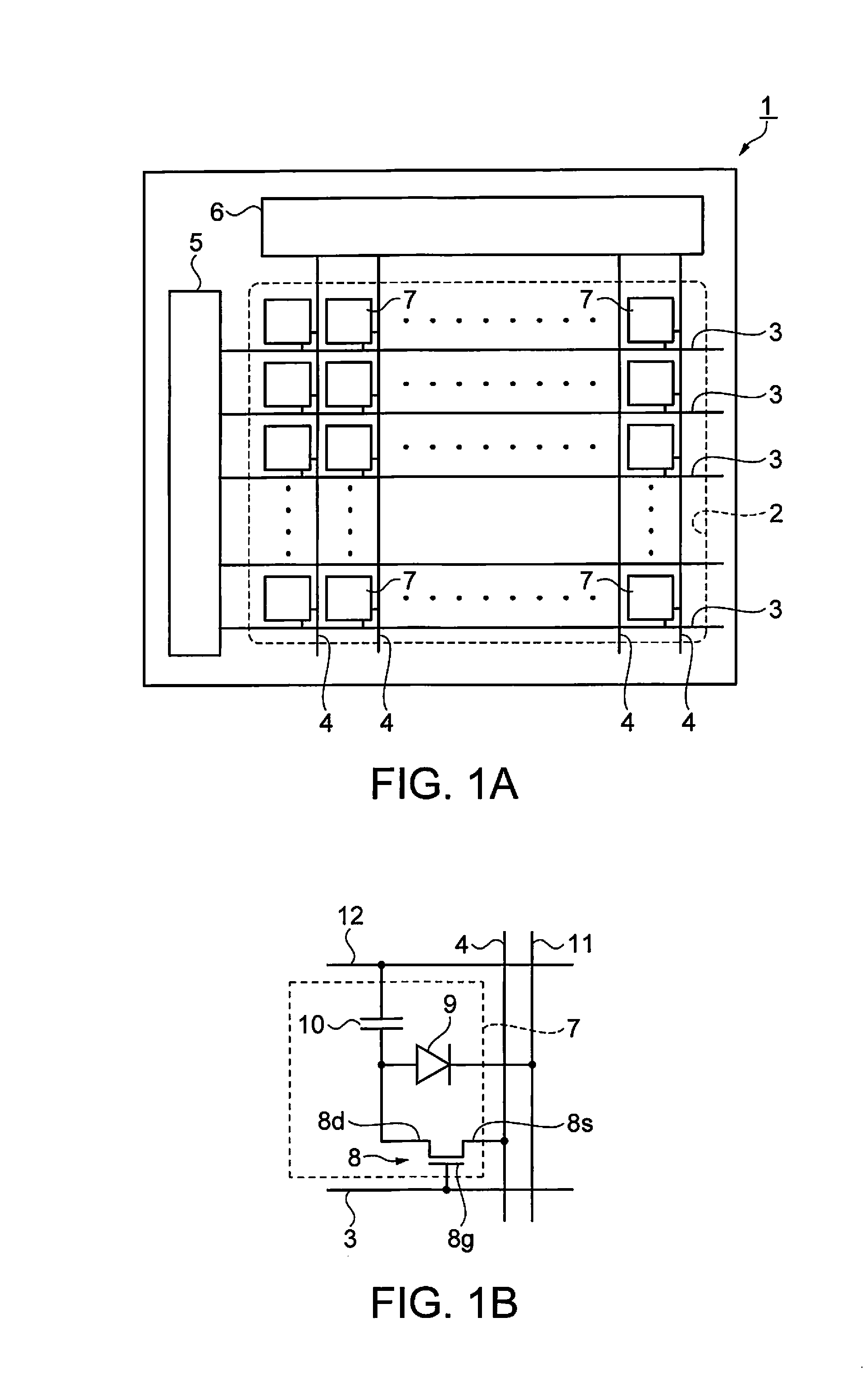
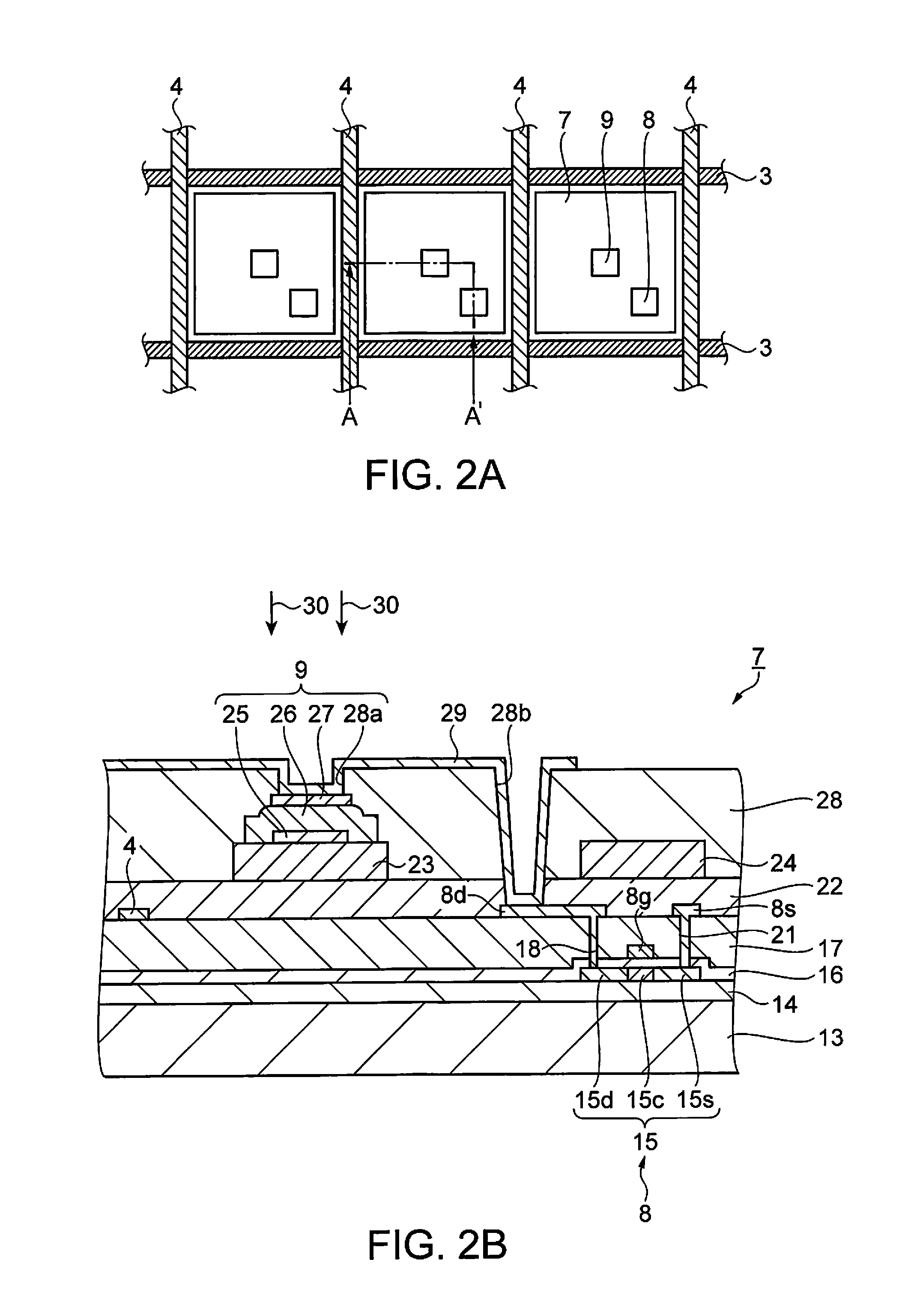
[0030]An image sensor relating to a first embodiment will be described in accordance with FIGS. 1 to 5. FIG. 1A is a schematic connection diagram showing an electrical configuration of the image sensor. FIG. 1B is an equivalent circuit diagram of a photo sensor. FIG. 2A is a schematic partial plan view showing the arrangement of photo sensors, and FIG. 2B is a schematic cross-sectional view showing the structure of a photo sensors along an A-A′ line in FIG. 2A. FIG. 3 is a schematic enlarged cross-sectional view showing a main section of the structure of a photo sensor.

[0031]As shown in FIG. 1A, an image sensor 1 serving as a photoelectric conversion apparatus of the present embodiment is provided with an element region 2. A plurality of scan lines 3 and a plurality of data lines 4 that extend and intersect each other are provided in the element region 2. A scan line circuit 5 serving as a drive part to which the plurality of scan lines 3 are electrically connected is provided to th...

second embodiment

[0061]Next, an embodiment of a photodiode will be described using a schematic enlarged cross-sectional view of FIG. 6 showing a main section of the structure of a photo sensor. The present embodiment differs from the first embodiment in that the third semiconductor layer 27 shown in FIG. 3 differs in shape. Note that, in subsequent embodiments including the present embodiment, the same reference signs are given to parts that are the same as the first embodiment, and description thereof may be omitted.

[0062]That is, in the present embodiment, as shown in FIG. 6, an image sensor 36 serving as a photoelectric conversion apparatus is provided with a photo sensor 37 serving as a photoelectric conversion element, and a photodiode 38 is provided in the photo sensor 37. In the photodiode 38, the first semiconductor layer 25, the second semiconductor layer 26 and the third semiconductor layer 39 are laminated on the lower electrode 23 in the stated order. The third semiconductor layer 39 is ...

third embodiment

[0065]Next, an embodiment of a photodiode will be described using a schematic enlarged cross-sectional view of FIG. 7 showing a main section of the structure of a photo sensor. The present embodiment differs from the first embodiment in that the third semiconductor layer 27 and the second semiconductor layer 26 shown in FIG. 3 are the same shape in plan view.

[0066]That is, in the present embodiment, as shown in FIG. 7, an image sensor 42 serving as a photoelectric conversion apparatus is provided with a photo sensor 43 serving as a photoelectric conversion element, and a photodiode 44 is provided in the photo sensor 43. In the photodiode 44, a lower electrode 45 is provided on the second interlayer insulation film 22, and an insulating layer 46, the first semiconductor layer 25, the second semiconductor layer 26, and a third semiconductor layer 47 are laminated on the lower electrode 45 in the stated order.

[0067]In the lower electrode 45, a place opposing the first semiconductor lay...


PUM


Abstract

A photoelectric conversion apparatus includes a substrate 13 and a photodiode 9 in which a first semiconductor layer 25, a second semiconductor layer 26 and a third semiconductor layer 27 are laminated on the substrate 13 in the stated order. The second semiconductor layer 26 is an i-type semiconductor layer, and one of the first semiconductor layer 25 and the third semiconductor layer 27 is an n-type semiconductor layer, and the other is a p-type semiconductor layer. Also, the first semiconductor layer 25 is covered by the second semiconductor layer 26.

Description

[0001]This application claims a priority to Japanese Patent Application No. 2014-054504 filed on Mar. 18, 2014 which is hereby expressly incorporated by reference in its entirety.BACKGROUND[0002]1. Technical Field[0003]Several aspects of the present invention relate to a photoelectric conversion apparatus and an electronic device.[0004]2. Related Art[0005]Photoelectric conversion apparatuses are used in apparatuses that capture two-dimensional images of a large high performance screen for medical use, apart from being used in electrical appliances such as facsimile machines and scanners. A photoelectric conversion apparatus in which photoelectric conversion parts are arranged two-dimensionally is disclosed in JP-A-2000-156522. According to JP-A-2000-156522, amorphous silicon semiconductor layers are used in the photoelectric conversion parts, with the layers being structured such that an i-type semiconductor layer is sandwiched between a p-type semiconductor layer and an n-type semi...

Claims


Application Information

Patent Timeline
IPC IPC(8): H01L31/105G06V40/145
CPCH01L31/105H01L27/14603H01L27/14612H01L27/14692G06V40/14G06V40/145G06V40/1341
Inventor JIROKU, HIROAKI
Owner SEIKO EPSON CORP
Learn More