Clock doubling circuit and method of operation
- Summary
- Abstract
- Description
- Claims
- Application Information
AI Technical Summary
Benefits of technology
Problems solved by technology
Method used
Image
Examples
Embodiment Construction
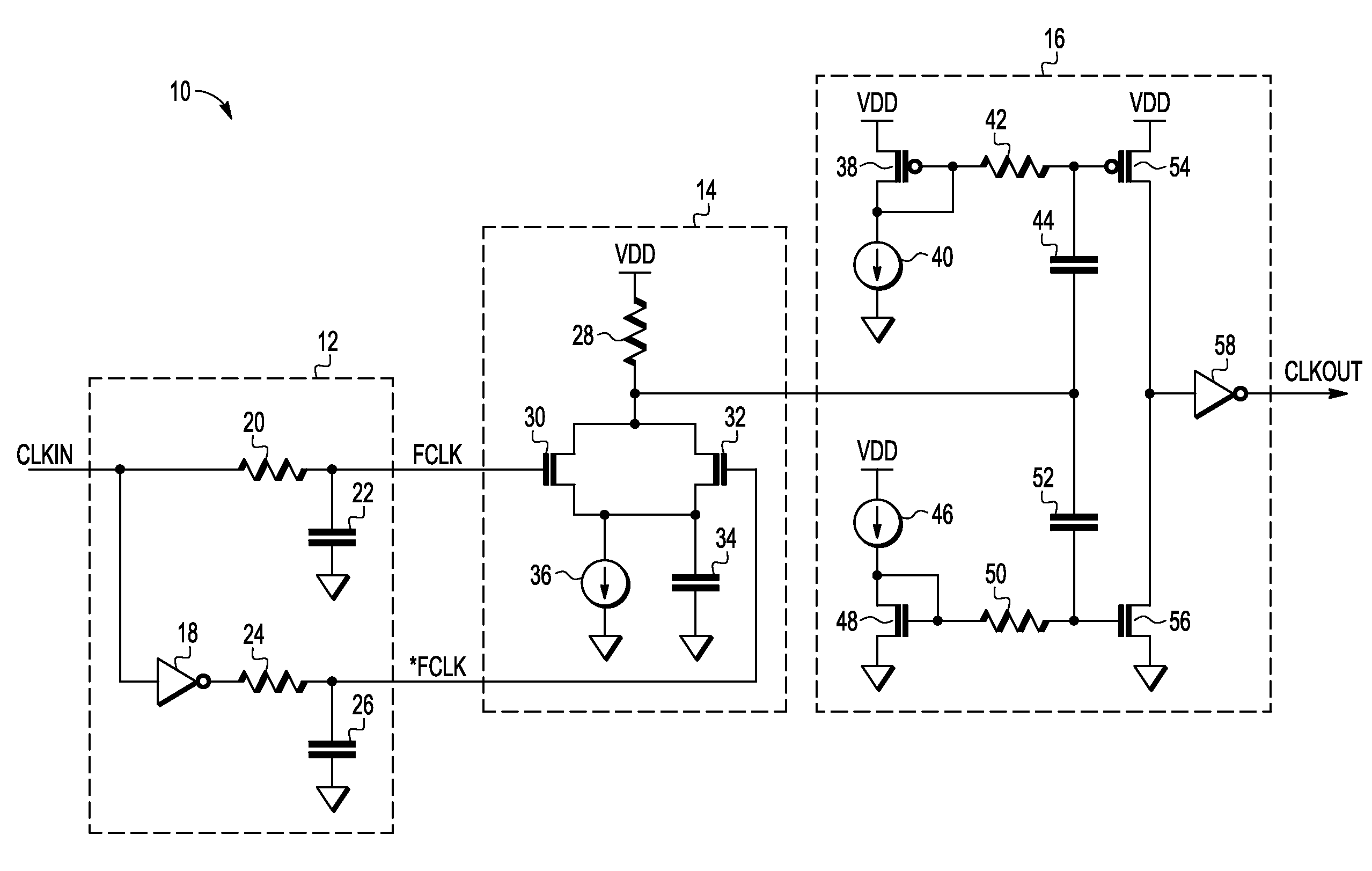
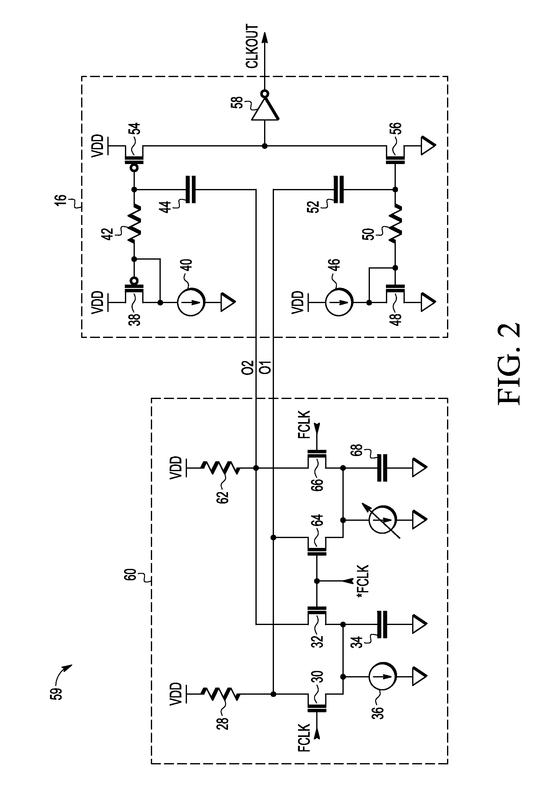
[0010]In one aspect, a frequency doubler converts a square wave clock to a filtered true and complementary clocks that have substantially slower transition times. The complementary clocks are used to generate a doubled clock that has slower transition times than the square wave clock. The doubled clock is then used to generate the doubled clock with transition times comparable to those of the square wave clock. This is better understood by reference to the drawings and the following written description.
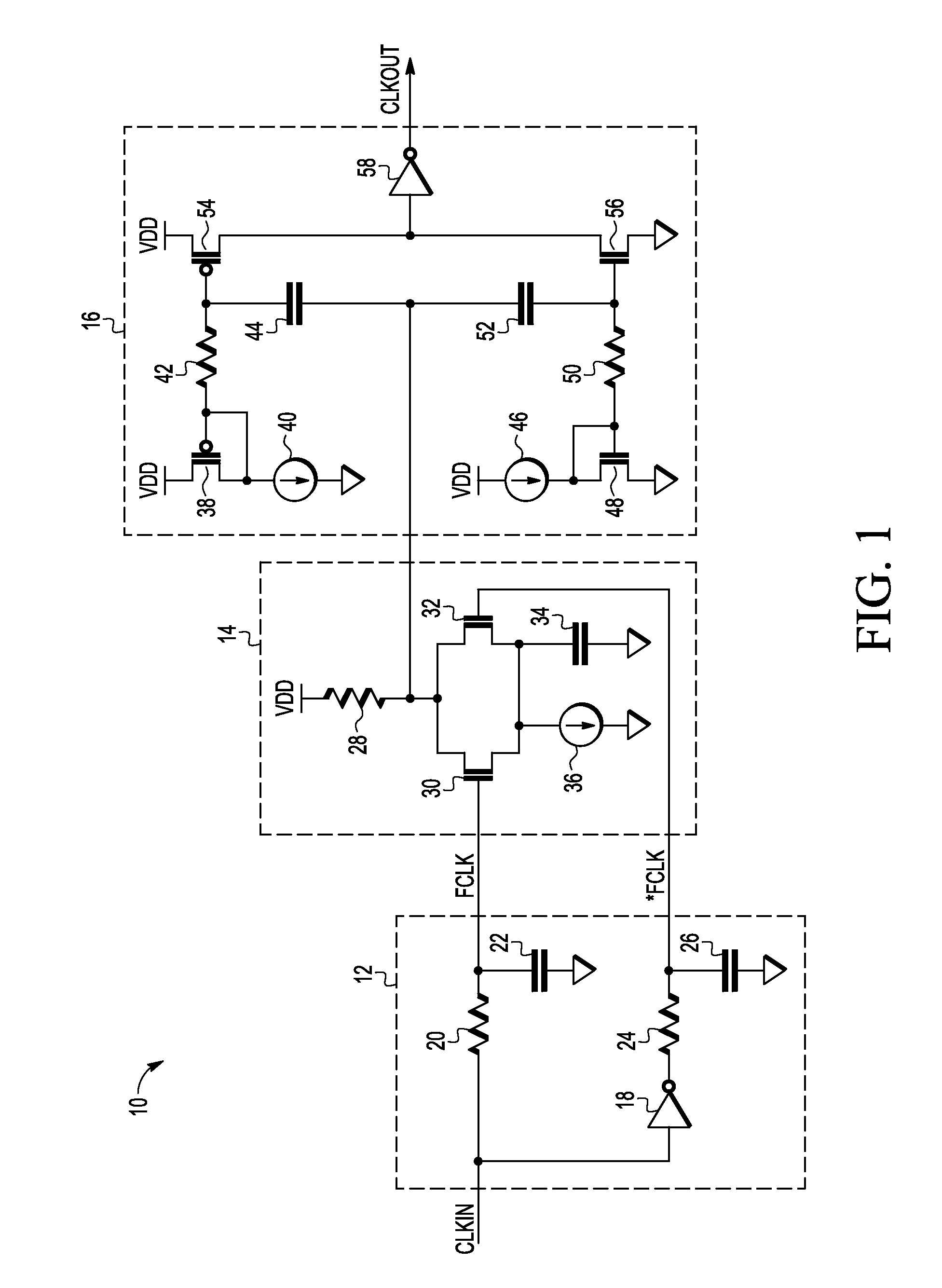
[0011]Shown in FIG. 1 is a clock doubler circuit 10 having a low pass filter 12, a frequency doubling circuit 14, and a clock shaping circuit 16. Low pass filter 12 has an inverter 18, a resistor 20, a capacitor 22, a resistor 24, and a capacitor 26. Inverter 18 has an input that receives an input clock Clkin and an output. Resistor 24 has an input connected to the output of inverter 18 and a second terminal. Capacitor 26 has a first terminal connected to the second terminal of resist...
PUM
 Abstract
Description
Claims
Application Information
 - R&D Engineer
- R&D Manager
- IP Professional
- Industry Leading Data Capabilities
- Powerful AI technology
- Patent DNA Extraction
Browse by: Latest US Patents, China's latest patents, Technical Efficacy Thesaurus, Application Domain, Technology Topic, Popular Technical Reports.
© 2024 PatSnap. All rights reserved.Legal|Privacy policy|Modern Slavery Act Transparency Statement|Sitemap|About US| Contact US: help@patsnap.com


