Static random access memory and fabrication methods thereof

a random access memory and random access technology, applied in the field of static random access memory and fabrication methods thereof, can solve the problems of unnecessarily re-creating the sram and the relatively complex fabrication of the existing stram structur

Active Publication Date: 2015-07-23
SEMICON MFG INT (SHANGHAI) CORP
View PDF13 Cites 5 Cited by
  • Summary
  • Abstract
  • Description
  • Claims
  • Application Information

AI Technical Summary

Benefits of technology

[0022]As shown in FIG. 3, the first bit line BL1, the second bit line BL2, and the first power source line Vdd in the first metal layer may extend along the y-axis direction. The word line WL and the second power source line Vss may extend along the x-axis direction. However, being limited by the layout of the semiconductor structures under the first metal layer and the second metal layer, the layout of the mask may have significantly high requirements for the fabrication process of the first metal layer and the second metal layer, especially for the first metal layer. For example, in the SRAMs with a 20 nm technology node, the minimum feature size of the patterns in the first metal layer may be only approximately 0.0039 μm2. Such a feature size may be way beyond the capability of the state-of-the-art fabrication process. Further, the layout of the first metal layer and the second metal layer may cause the pitch of the patterns in the second metal layer to be substantially small. For example, in the SRAMs with a 20 nm technology node, the minimum pitch of the patterns may be only approximately 88 nm. Such a small pitch may also beyond the capability of a single patterning process.

Problems solved by technology

Unlike dynamic random access memories (DRAM), it may only need to supply power to SRAM for storing data, and it may be unnecessarily to refresh the SRAM.
However, the fabrication of the existing STRAM structures may be relatively complex.

Method used


Image

  • Static random access memory and fabrication methods thereof
  • Static random access memory and fabrication methods thereof
  • Static random access memory and fabrication methods thereof

Examples


Embodiment Construction

[0017]Reference will now be made in detail to exemplary embodiments of the invention, which are illustrated in the accompanying drawings. Wherever possible, the same reference numbers will be used throughout the drawings to refer to the same or like parts.

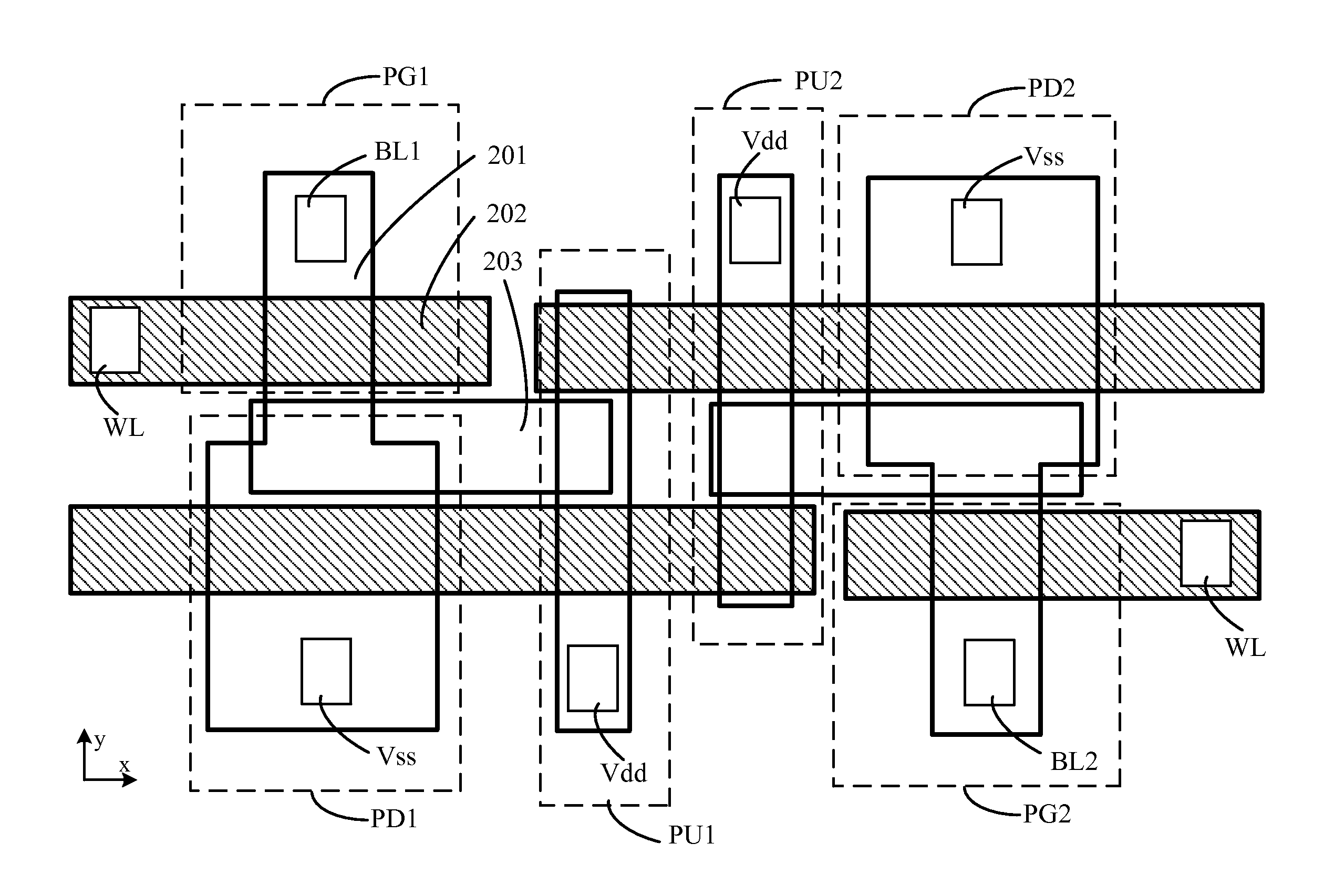
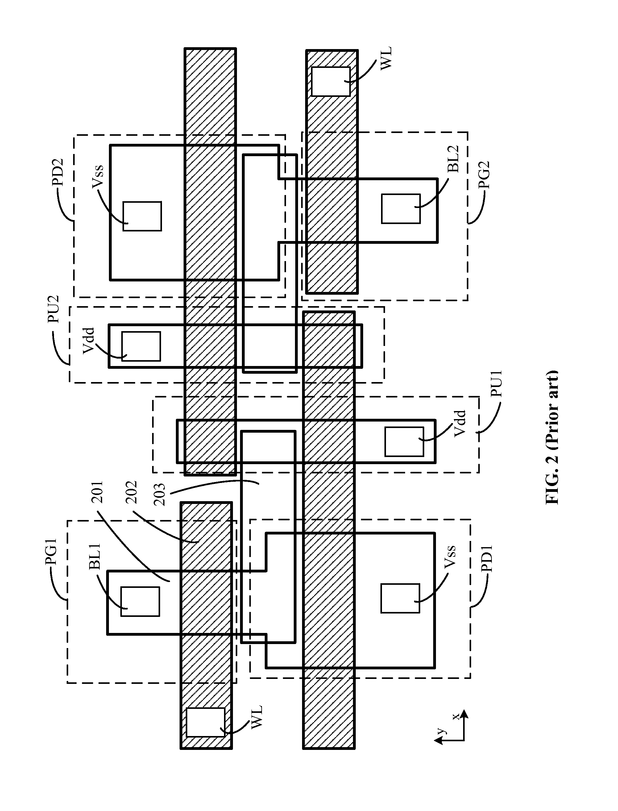
[0018]FIG. 2 illustrates the layout-design of an existing 6T random access memory (6T SRAM); and the layout-design illustrates a layout of an active region 201, a gate 202 and a metal structure 203.

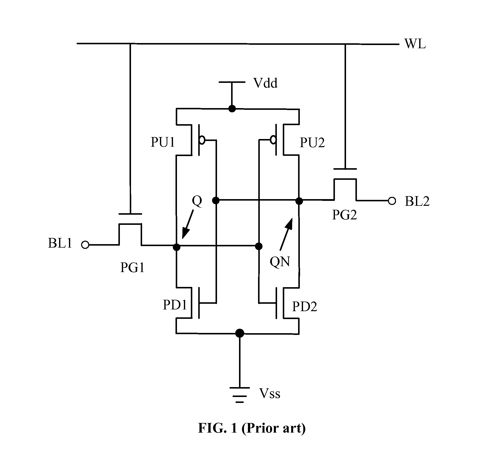
[0019]As shown in FIG. 2, the 6T SRAM may include a first pull-up transistor PU1, a second pull-up transistor PU2, a first pull-down transistor PD1, a second pull-down transistor PD2, a first transfer transistor PG1 and a second transfer transistor PG2. The first pull-up transistor PU1 and the first pull-down transistor PD1 may share a same gate 203; and the second pull-up transistor PU2 and the second pull-down transistor PD2 may share a same gate (not labeled). Further, the first transfer transistor PG1 and the first pull-down transist...


PUM


Abstract

A method for fabricating a static random access memory is provided. The method includes providing a semiconductor substrate. The method also includes forming a plurality of transistors on the semiconductor substrate. Further, the method includes forming a first metal layer having a word line electrically connecting with a partial number of the transistors. Further, the method also includes forming a second metal layer having a first bit line, a second bit line, a first power source line and second power source lines electrically connect with a partial number of the transistors.

Description

CROSS-REFERENCES TO RELATED APPLICATIONS[0001]This application claims the priority of Chinese patent application No. 201410025102.9, filed on Jan. 20, 2014, the entirety of which is incorporated herein by reference.FIELD OF THE INVENTION[0002]The present invention generally relates to the field of semiconductor technology and, more particularly, relates to static random access memories and fabrication methods thereof.BACKGROUND[0003]In applications of large scale integrations (LSIs), static random access memory (SRAM) are the widely-used on-chip memory. Unlike dynamic random access memories (DRAM), it may only need to supply power to SRAM for storing data, and it may be unnecessarily to refresh the SRAM. Therefore, SRAM may have advantages including high speed and low power consumption, etc.[0004]FIG. 1 illustrates a circuit structure of an existing SRAM, which may have six transistors (6T SRAM). As shown in FIG. 1, the 6T SRAM may include a first pull-up PMOS transistor PU1, a seco...

Claims


Application Information

Patent Timeline
Patent Type & Authority Applications(United States)
IPC IPC(8): H01L27/11
CPCH01L27/1104H01L27/0207H10B10/12
Inventor ZHANG, GONG
Owner SEMICON MFG INT (SHANGHAI) CORP
Why Eureka
Try Eureka