Dc/dc converter and display device
- Summary
- Abstract
- Description
- Claims
- Application Information
AI Technical Summary
Benefits of technology
Problems solved by technology
Method used
Image

Examples
example 1
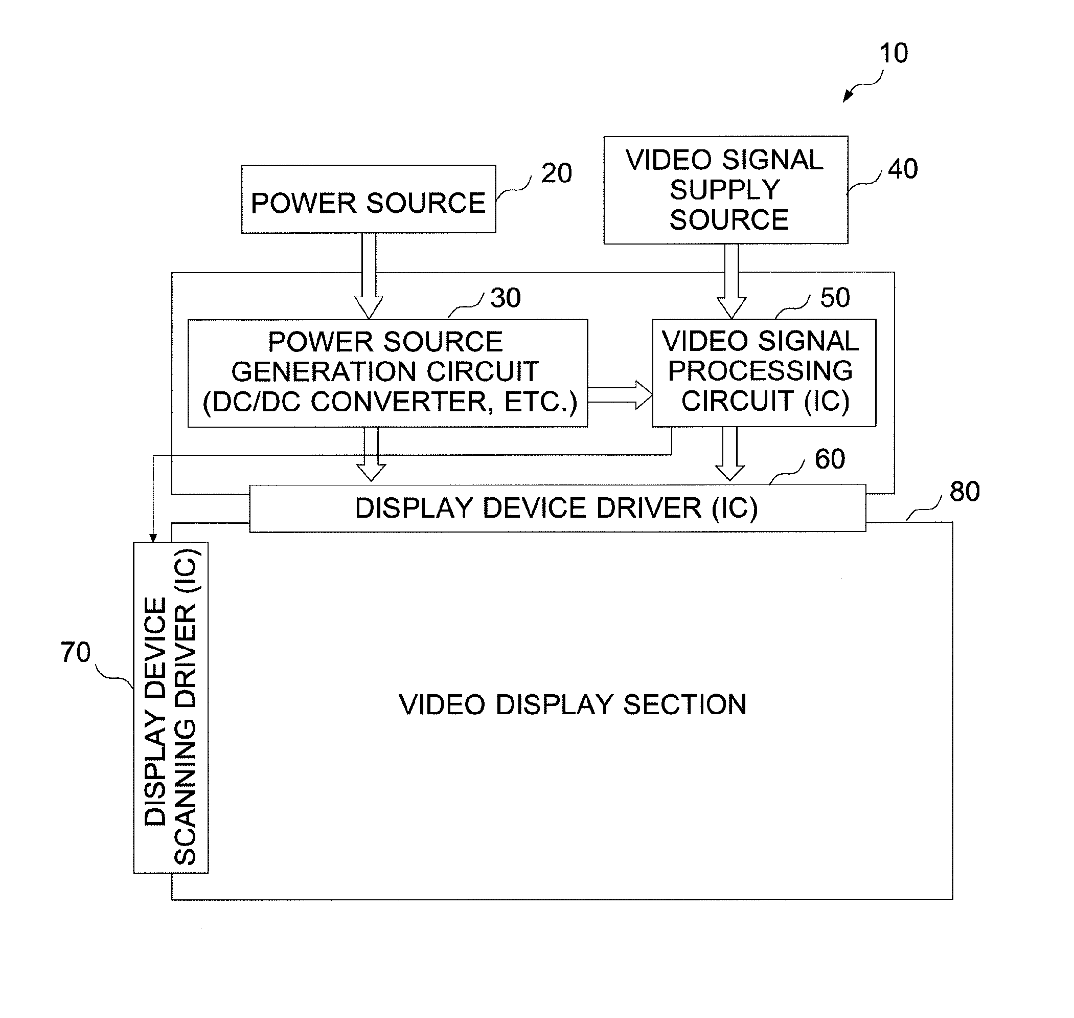
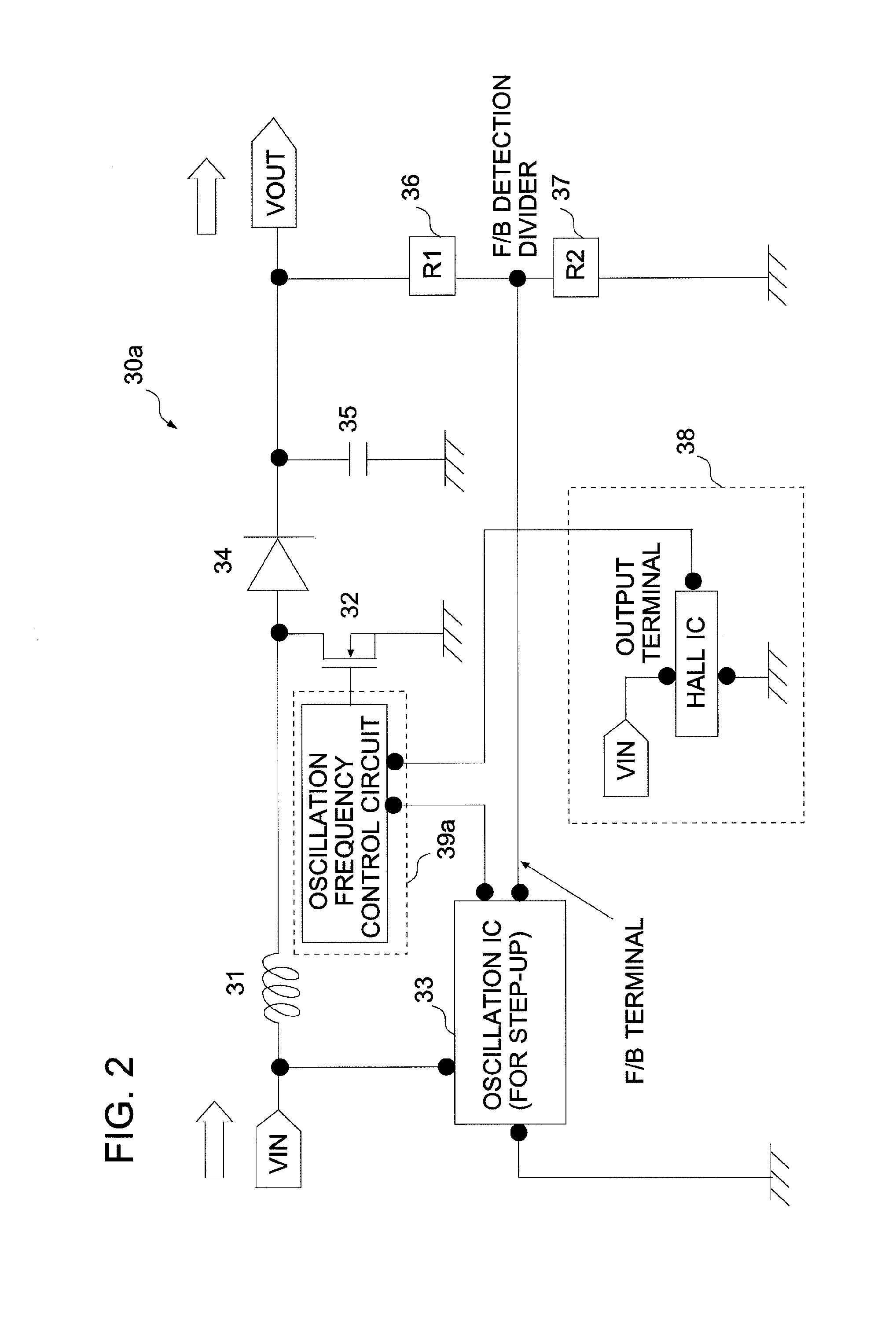
[0043]With reference to FIGS. 1-3, there will be given descriptions of a DC / DC converter and a display device according to the first example of the present invention, for illustrating the above embodiments of the present invention in detail. FIG. 1 is a block diagram showing a configuration of the display device of the present example. FIG. 2 is a block diagram showing a configuration of the DC / DC converter of the present example. In addition, FIGS. 3A-3D are diagrams showing control operations of the oscillation frequency in the DC / DC converter.
[0044]As shown in FIG. 1, the display device 10 of the present example includes: a power source 20 such as a battery; a power source generation circuit 30 such as a DC / DC converter; a video signal supply source 40 which supplies video signals; a video signal processing circuit 50 such as an IC for processing video signals; a display device driver 60 such as an IC for driving the display device; a display device scanning driver 70 such as an ...
example 2
[0059]Next, a DC / DC converter and a display device according to a second example of the present invention will be described now with reference to FIG. 4 and FIGS. 5A-5D. FIG. 4 is a block diagram showing a configuration of a DC / DC converter of the present example. FIGS. 5A-5D are diagrams showing control operations of an inductance in the DC / DC converter.
[0060]In the above first example, the activation of the latch circuit resulting from a decrease of the inductance value of the inductor 31 is suppressed by using the oscillation frequency control circuit 39a as a strong magnetic field existence latch operation avoidance circuit and by increasing the oscillation frequency used for driving the switching FET 32 in a strong magnetic field. However, in the present example, the activation of a latch circuit is suppressed by controlling the inductance. Specifically, there is employed an inductance control circuit including: a second switching element; a second inductor which is connected t...
example 3
[0072]Next, a DC / DC converter and a display device according to a third example of the present invention will be described now with reference to FIG. 6 and FIGS. 7A-7D. FIG. 6 is a block diagram showing a configuration of the DC / DC converter of the present example. FIGS. 7A-7 D are diagrams showing control operations of the feedback voltage in the DC / DC converter.
[0073]In the above first example, the activation of the latch circuit resulting from a decrease in the inductance value of the inductor 31 is suppressed by increasing the oscillation frequency used for driving the switching FET 32 in a strong magnetic field. In the second example, the activation of the latch circuit is suppressed by increasing the value of the inductance in a strong magnetic field. However, in this example, the activation of the latch circuit is suppressed by controlling the feedback voltage. To be more precise, there is provided a feedback voltage control circuit including: a resistance whose one end is co...
PUM
 Abstract
Description
Claims
Application Information
 - R&D
- Intellectual Property
- Life Sciences
- Materials
- Tech Scout
- Unparalleled Data Quality
- Higher Quality Content
- 60% Fewer Hallucinations
Browse by: Latest US Patents, China's latest patents, Technical Efficacy Thesaurus, Application Domain, Technology Topic, Popular Technical Reports.
© 2025 PatSnap. All rights reserved.Legal|Privacy policy|Modern Slavery Act Transparency Statement|Sitemap|About US| Contact US: help@patsnap.com