
Method for performing built-in self-tests and electronic circuit

a self-testing and electronic circuit technology, applied in the field of vlsi chip testing, can solve the problems of supply voltage fluctuations, significant electrical power consumption of abist, etc., and achieve the effect of reducing current fluctuations

Inactive Publication Date: 2015-06-11
IBM CORP
View PDF10 Cites 2 Cited by
  • Summary
  • Abstract
  • Description
  • Claims
  • Application Information

AI Technical Summary

Benefits of technology

The patent describes a method to reduce current fluctuations that can cause malfunctions in electronic circuits. This is achieved by delaying the starting time of the array built-in self-test engines based on the delay value determined for each memory array. The delay value is determined based on the test duration of each memory array and the maximum test duration of all memory arrays. The at least one programmable delay unit controls the array built-in self-test engine start so that at least subsets of the engines start at different points of time. This method reduces the current fluctuations and ensures the proper functioning of electronic circuits.

Problems solved by technology

Due to the rising complexity of memory, ABIST consumes a significant electrical power.
When starting the ABIST, there is a sudden large current draw from the electronic circuit power supply leading to fluctuations of the supply voltage.

Method used


Image

  • Method for performing built-in self-tests and electronic circuit
  • Method for performing built-in self-tests and electronic circuit
  • Method for performing built-in self-tests and electronic circuit

Examples


first embodiment

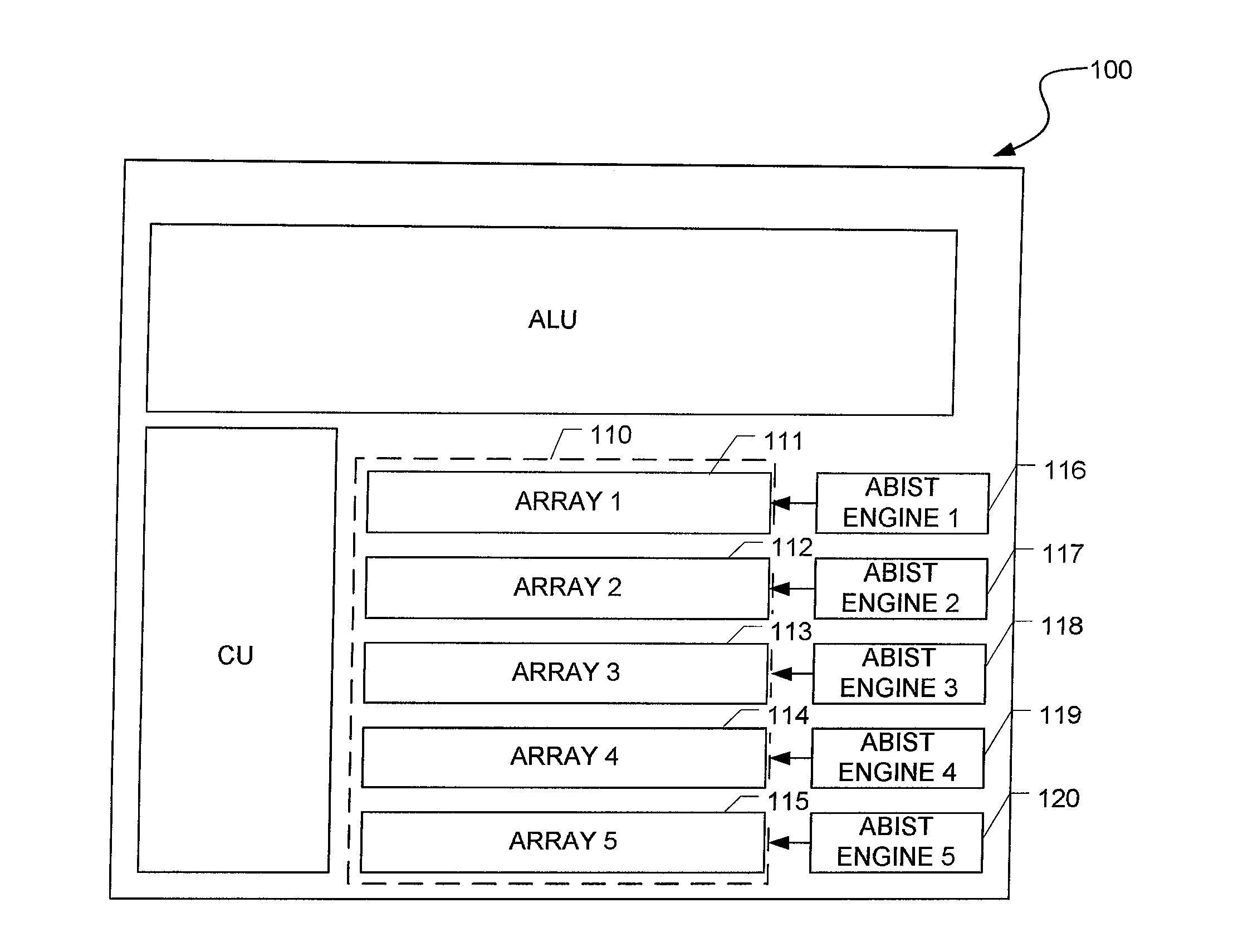
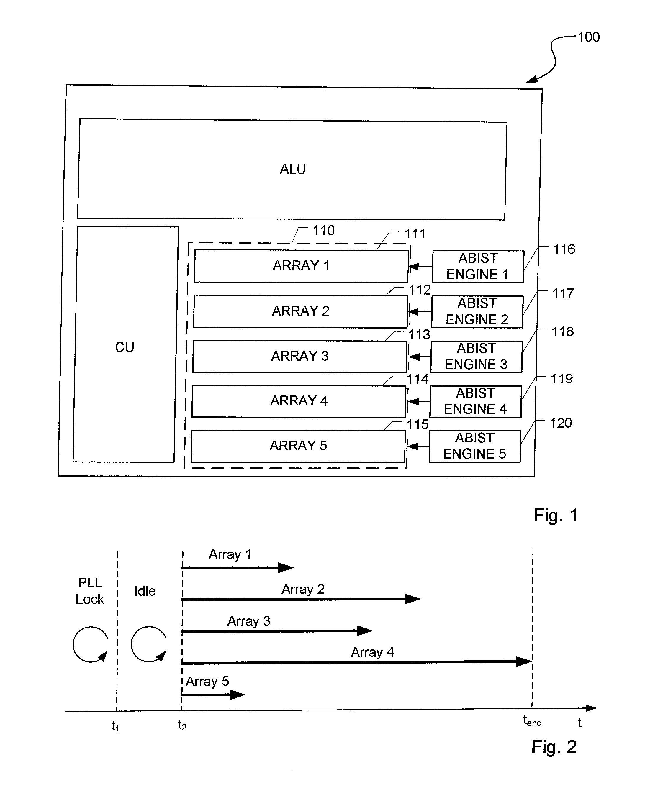
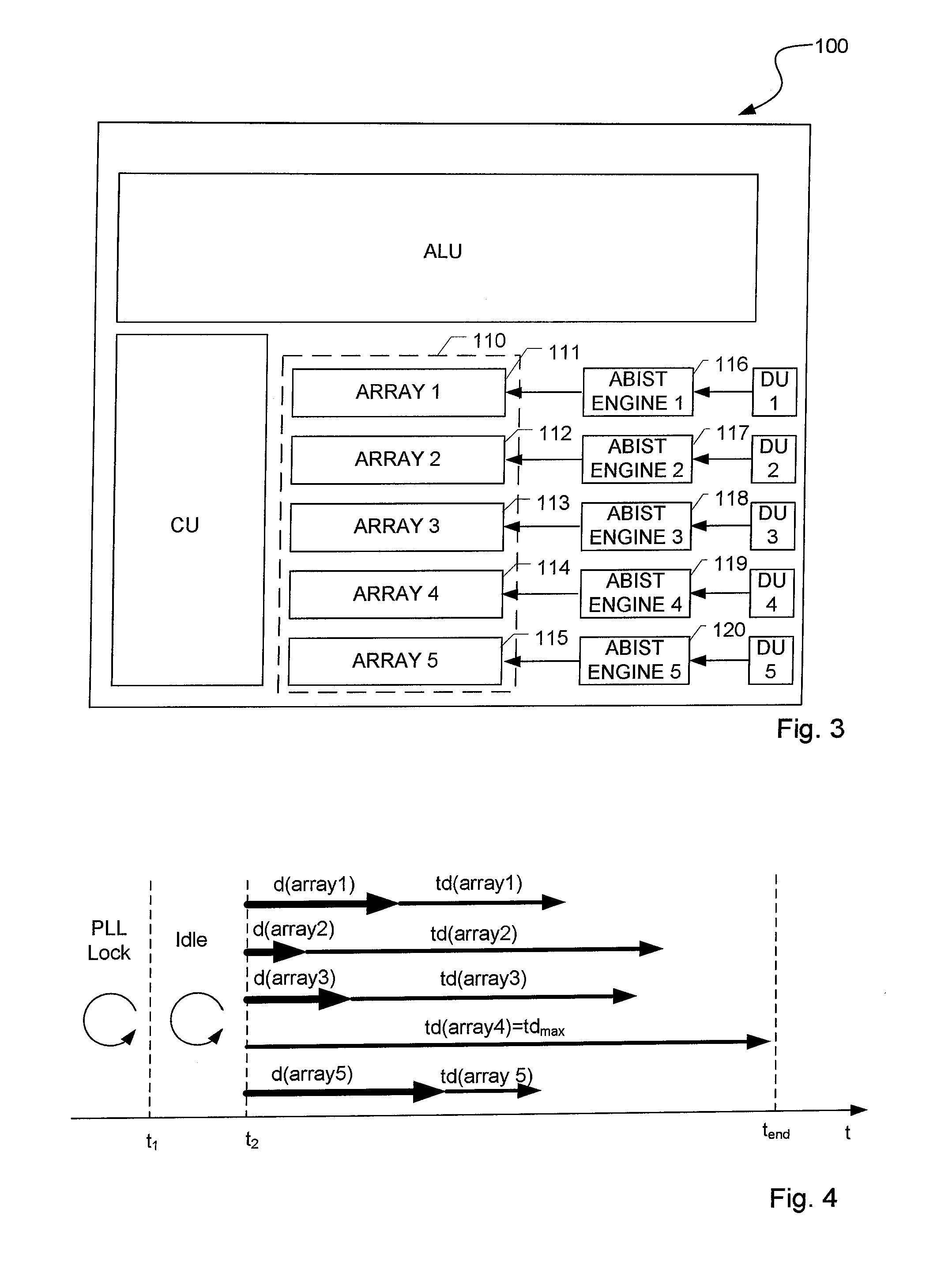
[0048]FIG. 4 shows a schematic flow chart of performing ABIST according to a According to the demonstrated example, the electronic circuit 100 comprises five memory arrays to be tested. It is worth mentioning that the electronic circuit 100 is not limited to said number of memory arrays, i.e. may comprise more or less than five memory arrays. In addition, each memory array may be formed by a set of memory sub-arrays to be tested by a common ABIST engine. As indicated above, after starting the test, a first procedure, so-called PLL lock, may be performed. After finishing the first procedure (point of time t1), a second procedure (Idle) may be performed during which the phase locked clock is provided to the memory arrays 111-115. After finishing the second procedure (point of time t2), the ABIST procedures of the respective memory arrays may be started consecutively.

[0049]Preferably, before starting the ABIST procedures, the test durations of all memory arrays are determined. The tes...

second embodiment

[0052]FIG. 5 shows a schematic flow chart of performing ABIST according to a second, preferred embodiment. According to said second embodiment, the delay values for delaying the start ABIST engines are chosen such that all ABIST engines 116-120 stop at the same point of time, namely at the point of time at which the longest running ABIST engine terminates (tend). The delay value for delaying the start of an ABIST engine may be calculated based on the longest test duration tdmax and the test duration of the memory array said ABIST engine is correlated with. Specifically, the delay duration may be calculated based on the following formula:

dn=tdmax−tdn;

wherein dn is the delay value correlated to memory array n, tdmax is the period of time which is needed by the longest running ABIST engine for performing ABIST procedure and tdn is the period of time which is needed for performing ABIST procedure of memory array n, wherein n is an integer, n [1;N] and N is the number of memory arrays co...


PUM


Abstract

The invention relates to a method for performing an array built-in self-test (ABIST) on an electronic circuit (100), the electronic circuit (100) comprising a memory (110) with at least two memory arrays (111-115) and at least two array built-in self-test engines (116-120), wherein each automatic built-in self-test engine (116-120) is associated with a different memory array (111-115) and wherein each array built-in self-test engine (116-120) is associated with a programmable delay unit (DU1-DU5), the method comprising the following steps:determine at least one delay value (dn), the delay value (dn) corresponding to an array built-in self-test engine (116-120) and the delay value (dn) depending on the execution time (tdn) for testing the memory array (111-115) associated with the array built-in self-test engine (116-120);provide the at least one delay value (dn) to the programmable delay unit (DU1-DU5); and delay the start of the array built-in self-test engine (116-120) depending on the respective delay value (dn).

Description

FIELD OF THE INVENTION[0001]The present invention relates generally to the field of VLSI Chip testing. More specifically, the present invention is related to a method for performing array built-in self-tests and an electronic circuit comprising array built-in self-test engines.BACKGROUND[0002]Generally, a built-in self-test (BIST) is a mechanism that permits a machine to test a circuitry on its own or independently. Besides other applications, built-in self-tests are used in electronic circuits for testing the functionality of modules or subunits of the electronic circuit or the whole electronic circuit. In other words, the electronic circuit provides a function that verifies all or a portion of the internal functionality of the electronic circuit. The main purpose of BIST is to decrease the test time, reduce the complexity of external test equipment, and thereby decrease the testing costs.[0003]Array built-in self-test (ABIST) is used to test memory arrays that are contained in ele...

Claims


Application Information

Patent Timeline
Patent Type & Authority Applications(United States)
IPC IPC(8): G11C29/12
CPCG11C29/12015G01R31/2856G01R31/3004G01R31/31701G01R31/31721G01R31/3187G06F1/3275G06F1/3287G06F11/1068G06F11/2236G06F11/27G11C29/26G11C29/50G11C2029/0401G11C2029/2602G11C2029/3202G11C2029/3602
Inventor ECKERT, MARTINTORREITER, OTTOZOELIN, CHRISTIAN
Owner IBM CORP
Learn More