Display panel
a display panel and panel technology, applied in non-linear optics, instruments, optics, etc., can solve the problems of inability to adjust, damage to electronic components inside electronic products, and difficulty in fabrication processes, so as to improve the ability against an esd effect
- Summary
- Abstract
- Description
- Claims
- Application Information
AI Technical Summary
Benefits of technology
Problems solved by technology
Method used
Image


Examples
first embodiment
[0021]FIG. 1 is a schematic top view of a display panel according to the invention. FIG. 2 is a schematic cross-sectional view of the display panel of FIG. 1 along line I-I′.
[0022]Referring to FIG. 1 and FIG. 2, a display panel 100 includes a display region 102 and a non-display region 104 surrounding the display region 102. The display panel 100 is a FFS LCD panel, for example. In the following embodiments of the invention, the display panel 100 is a FFS LCD panel for illustration purposes. The display panel 100 includes a color filter substrate 110, a pixel array substrate 120 opposite to the color filter substrate 110, a conductive structure 130, a sealant 140, and a display medium 150.
[0023]The color filter substrate 110 includes a first substrate 112, a black matrix layer 114, an electrostatic protection layer 116, a color filter layer 118, and a planarization layer 119.
[0024]A material of the first substrate 112 includes glass, quartz, organic polymers, or other suitable mater...
second embodiment
[0039]FIG. 3 is a schematic top view of a display panel according to the invention. FIG. 4 is a schematic cross-sectional view of the display panel of FIG. 3 along line I-I′. The embodiment of FIG. 3 and FIG. 4 is similar to the afore-mentioned embodiment of FIG. 1 and FIG. 2, wherein identical or similar elements are denoted by identical or similar reference numerals. Description of the same elements will be omitted hereinafter, and only the differences will be explained below. Please refer to FIG. 3 and FIG. 4, the embodiment of FIG. 3 and FIG. 4 is similar to the afore-mentioned embodiment of FIG. 1 and FIG. 2, and one of the differences is that the electrostatic protection layer 216 is only located on the entire second surface 114b of the black matrix layer 114. Namely, in the display panel 200, the electrostatic protection layer 216 of the color filter substrate 110 is not located in the first openings 114a. Thus, a portion of the electrostatic protection layer 216 is at least ...
third embodiment
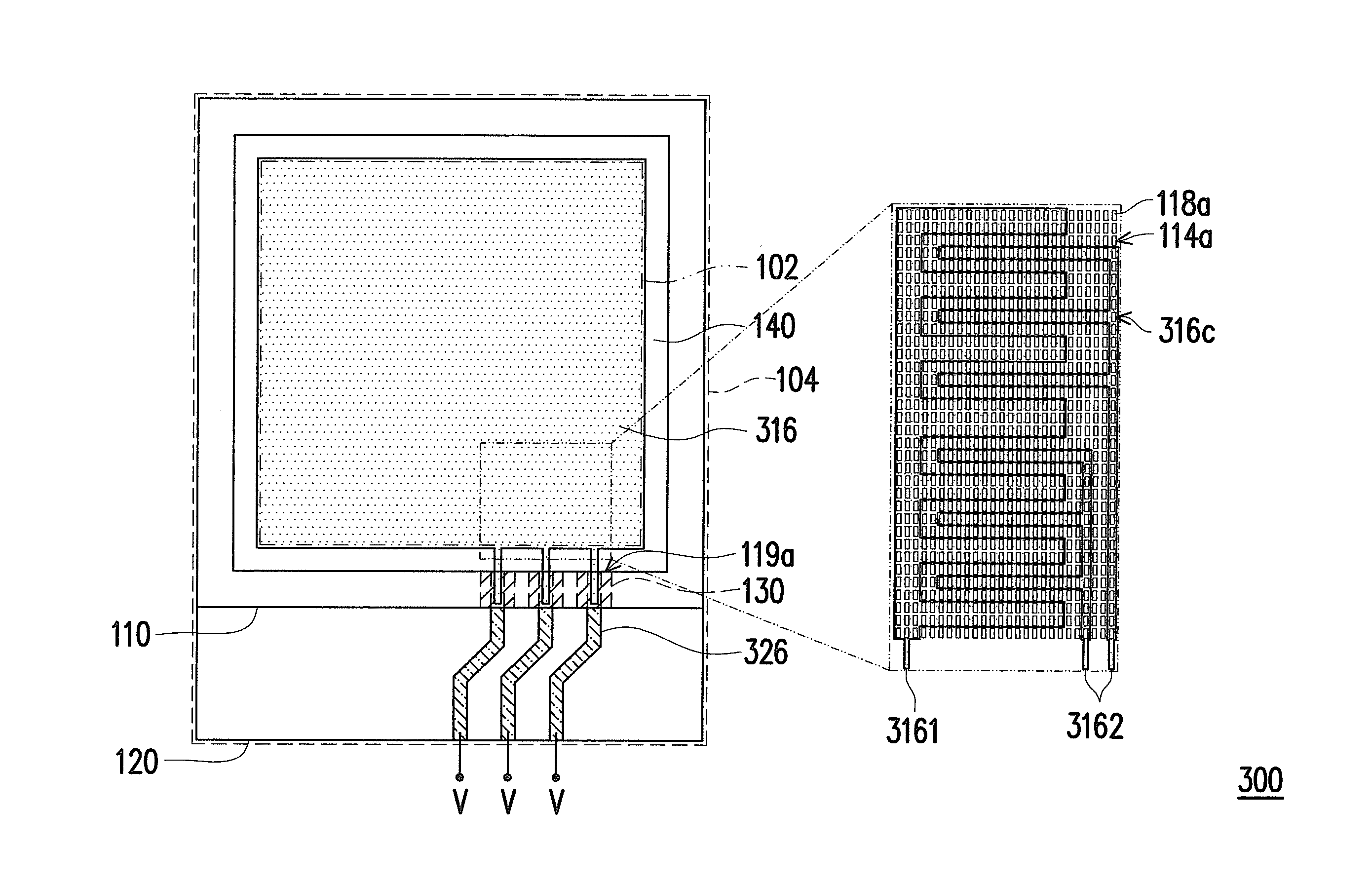
[0043]FIG. 6 is a schematic top view of a display panel according to the invention. FIG. 7A is a schematic partial top view of a first electrode and a second electrode of FIG. 6. FIGS. 7B and 7C is schematic partial top views of a first electrode and a second electrode according to other embodiments of the invention.
[0044]The embodiment of FIG. 6 and FIG. 7A is similar to the afore-mentioned embodiment of FIG. 3 and FIG. 4, wherein identical or similar elements are denoted by identical or similar reference numerals. Description of the same elements will be omitted hereinafter, and only the differences will be explained below. Please refer to FIG. 6 and FIG. 7A, the embodiment of FIG. 6 and FIG. 7A is similar to the afore-mentioned embodiment of FIG. 3 and FIG. 4, and one of the differences is that the electrostatic protection layer 316 includes at least one first electrode 3161 and at least one second electrode 3162, and the display panel 300 includes at least one conductive structu...
PUM
 Abstract
Description
Claims
Application Information
 - R&D
- Intellectual Property
- Life Sciences
- Materials
- Tech Scout
- Unparalleled Data Quality
- Higher Quality Content
- 60% Fewer Hallucinations
Browse by: Latest US Patents, China's latest patents, Technical Efficacy Thesaurus, Application Domain, Technology Topic, Popular Technical Reports.
© 2025 PatSnap. All rights reserved.Legal|Privacy policy|Modern Slavery Act Transparency Statement|Sitemap|About US| Contact US: help@patsnap.com