Semiconductor device and method of manufacturing the same

Inactive Publication Date: 2015-03-05
TOYOTA JIDOSHA KK
View PDF3 Cites 10 Cited by
  • Summary
  • Abstract
  • Description
  • Claims
  • Application Information

AI Technical Summary

Benefits of technology

The present invention provides a technique for preventing bubbles from forming in joint materials when joining semiconductor chips to other members using joint materials. This is achieved by ensuring that the tensile force applied to the semiconductor chip from the joint material at the melting temperature of the joint material is equal to the tensile force applied to the other surface of the semiconductor chip from the other electrode. This technique helps to create a more stable and reliable joint between the semiconductor chip and the other member.

Problems solved by technology

If the bubble is mixed during solder joining, solder joining is carried out with the bubble remaining in the solder, and this may affect an electrical characteristic of the semiconductor device.

Method used


Image

  • Semiconductor device and method of manufacturing the same
  • Semiconductor device and method of manufacturing the same
  • Semiconductor device and method of manufacturing the same

Examples


first embodiment

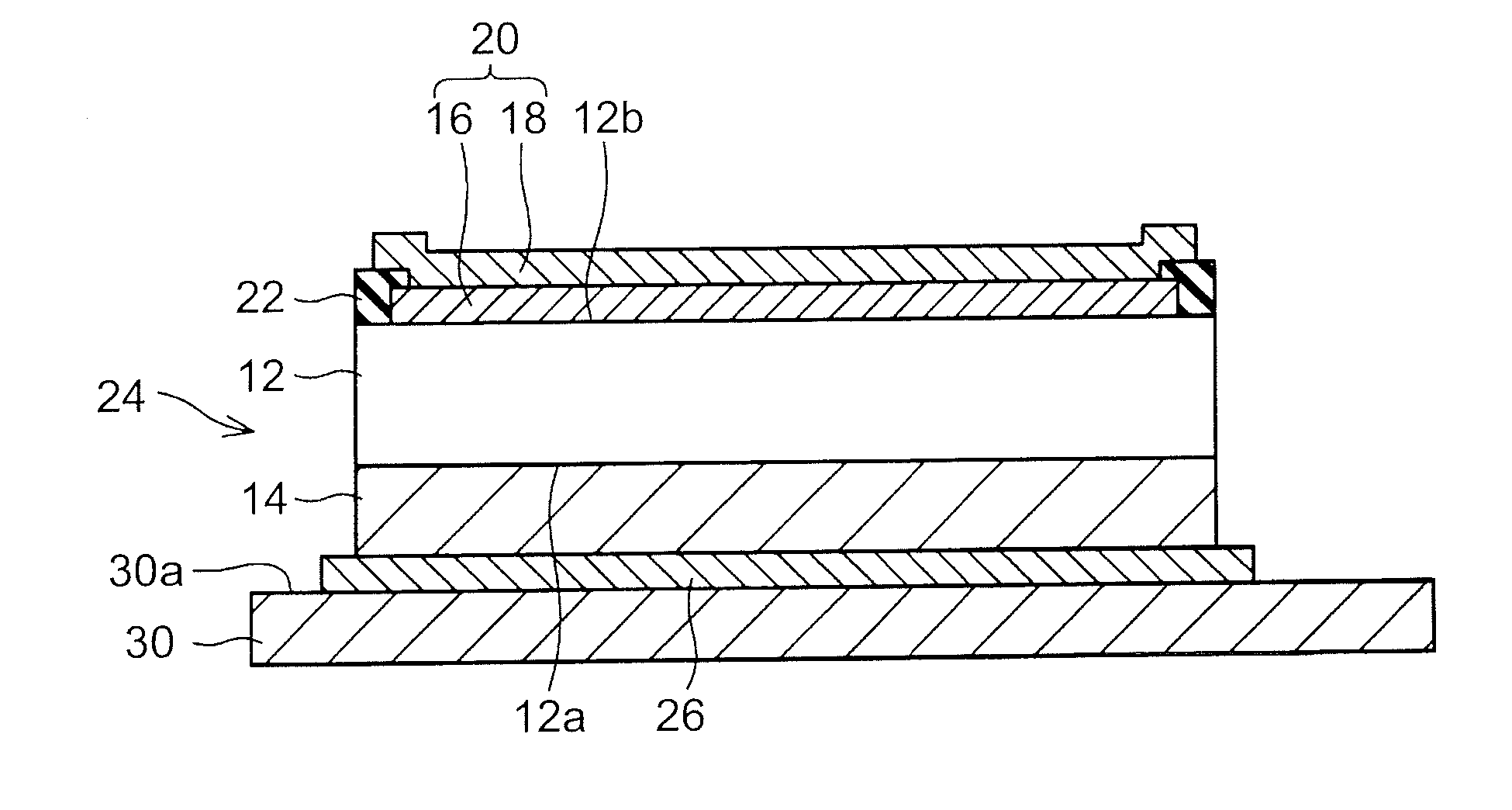
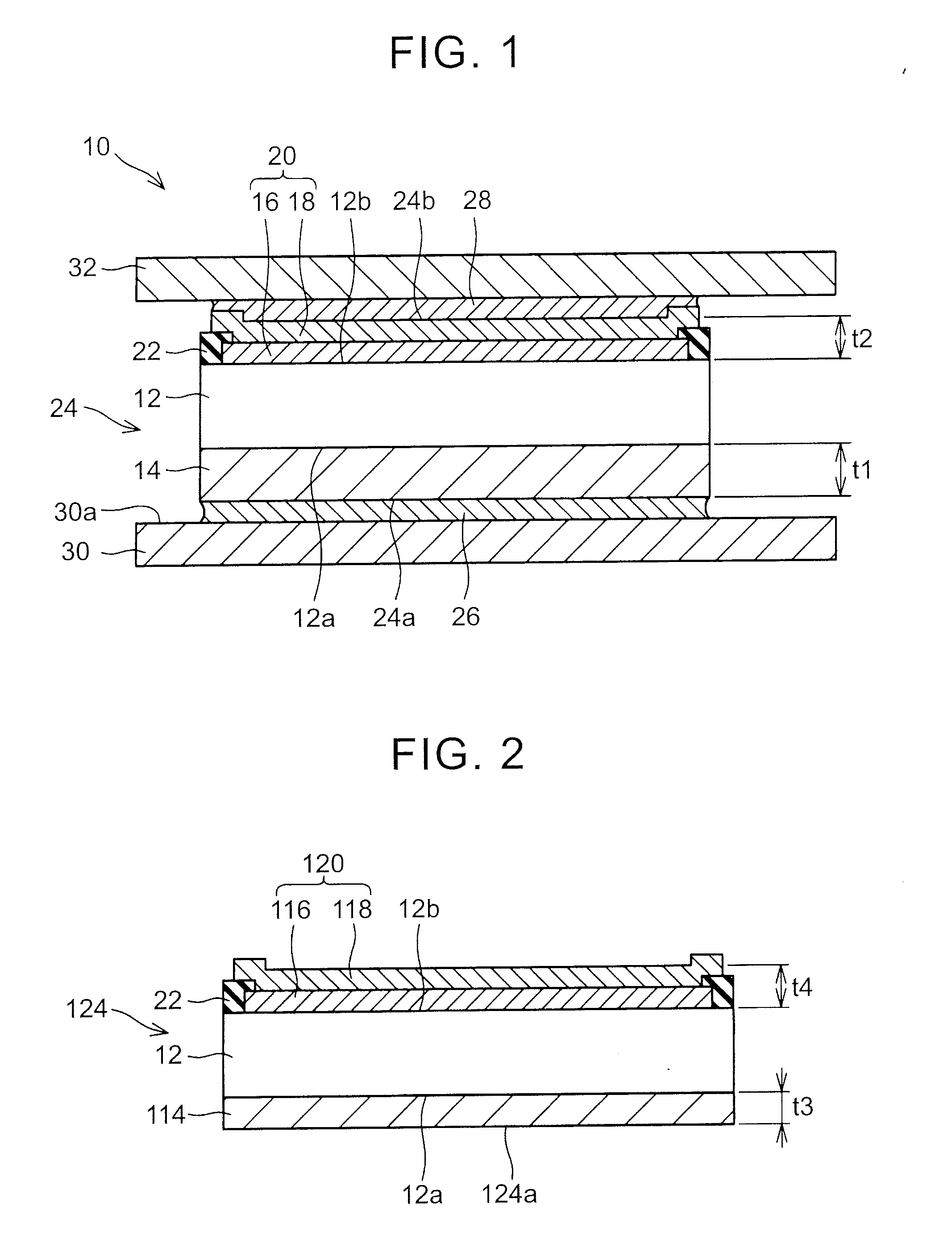
[0054]In other words, in the first embodiment, the volume of the back surface electrode 14 is set to be larger than the volume of the metal electrode 20, and the tensile force that is generated by the back surface electrode 14 is thereby set to be larger than the tensile force that is generated by the metal electrode 20. Meanwhile, in this embodiment, the effective linear expansion coefficient of the back surface electrode 214 is set to be larger than the effective linear expansion coefficient of the metal electrode 220, and the tensile force that is generated by the back surface electrode 214 is thereby set to be larger than the tensile force that is generated by the metal electrode 220.

[0055]Next, a description will be made on a third embodiment with reference to FIG. 6. A description will hereinafter be made only on points that differ from the first embodiment, and a detailed description on the same configuration as that of the first embodiment will not be made.

[0056]In a semicon...

fourth embodiment

[0065]The semiconductor device that includes the semiconductor chip 424 of the fourth embodiment can be manufactured in substantially the same manufacturing method of the above-described semiconductor device 10. However, the manufacturing method differs from that of the semiconductor device 10 in the following points. More specifically, in the semiconductor device that includes the semiconductor chip 424, the front surface electrode 418 is manufactured by the mask sputtering method. In other words, the non-electrolytic plating method is not used. It is possible by using the mask sputtering method to form the front surface electrode 418 as the continuous and seamless metal film not only on the exposed surfaces of the front surface electrodes 416a, 416b but also the front surface of the insulation layer 422. In addition, the materials that are used to constitute the front surface electrode 418 have smaller linear expansion coefficients than the materials that constitute the front surf...


PUM


Abstract

A semiconductor device includes a semiconductor chip and a joined member. The semiconductor chip has a semiconductor substrate, a first electrode, and a second electrode. The first electrode is arranged on a first surface of the semiconductor substrate. The second electrode is arranged on a second surface of the semiconductor substrate. The first electrode is joined to the joined member via a joint material. A tensile force in a surface direction of the first surface that is applied to the first surface of the semiconductor substrate from the first electrode due to thermal expansion of the first electrode at a melting temperature of the joint material is at least equal to a tensile force in the surface direction that is applied to the second surface of the semiconductor substrate from the second electrode due to thermal expansion of the second electrode at the melting temperature.

Description

INCORPORATION BY REFERENCE[0001]The disclosure of Japanese Patent Application No. 2013-181409 filed on Sep. 2, 2013 including the specification, drawings and abstract is incorporated herein by reference in its entirety.BACKGROUND OF THE INVENTION[0002]1. Field of the Invention[0003]The present invention relates to a semiconductor device and a method of manufacturing the same.[0004]2. Description of Related Art[0005]A semiconductor device has been known in which a connection conductor and the like are joined to a semiconductor chip by soldering. For example, a semiconductor device disclosed in Japanese Patent Application Publication No. 2005-051084 (JP 2005-051084 A) includes a semiconductor chip and a lead frame (an example of the connection conductor). The semiconductor chip includes a semiconductor substrate, a front surface electrode that is formed on a front surface of the semiconductor substrate, and a back surface electrode that is formed on a back surface of the semiconductor...

Claims


Application Information

Patent Timeline
IPC IPC(8): H01L23/00H01L23/485H01L21/28H01L23/495
CPCH01L23/564H01L21/28H01L23/485H01L23/49562H01L23/49513H01L24/33H01L24/83H01L2924/13055H01L2924/13091H01L23/051H01L2224/05078H01L23/4827H01L24/03H01L24/05H01L24/06H01L24/29H01L24/32H01L2224/0345H01L2224/03464H01L2224/04026H01L2224/05016H01L2224/05022H01L2224/05073H01L2224/05083H01L2224/05084H01L2224/05124H01L2224/05155H01L2224/05166H01L2224/05558H01L2224/05562H01L2224/05571H01L2224/05573H01L2224/05644H01L2224/0603H01L2224/06051H01L2224/06181H01L2224/06505H01L2224/291H01L2224/32245H01L2224/33181H01L2224/83192H01L2224/8321H01L2224/83447H01L2224/83815H01L2924/3511H01L2224/05568H01L2224/05023H01L2224/05584H01L2924/00H01L2924/00014H01L2924/014H01L2924/00012
Inventor NARITA, KATSUTOSHI
Owner TOYOTA JIDOSHA KK
Why Eureka
Try Eureka