Semiconductor device
a semiconductor and display device technology, applied in semiconductor devices, digital storage, instruments, etc., can solve the problems of difficult to prolong a period, difficult to increase the driving frequency of the driver circuit, and charge leaked from the gate of the transistor mb>1/b>, so as to achieve the effect of reducing the w/l of the transistor
- Summary
- Abstract
- Description
- Claims
- Application Information
AI Technical Summary
Benefits of technology
Problems solved by technology
Method used
Image
Examples
embodiment 1
[0041]In this embodiment, a basic circuit, a sequential circuit including the basic circuit, and a shift register circuit including the sequential circuit which are embodiments of the present invention will be described.
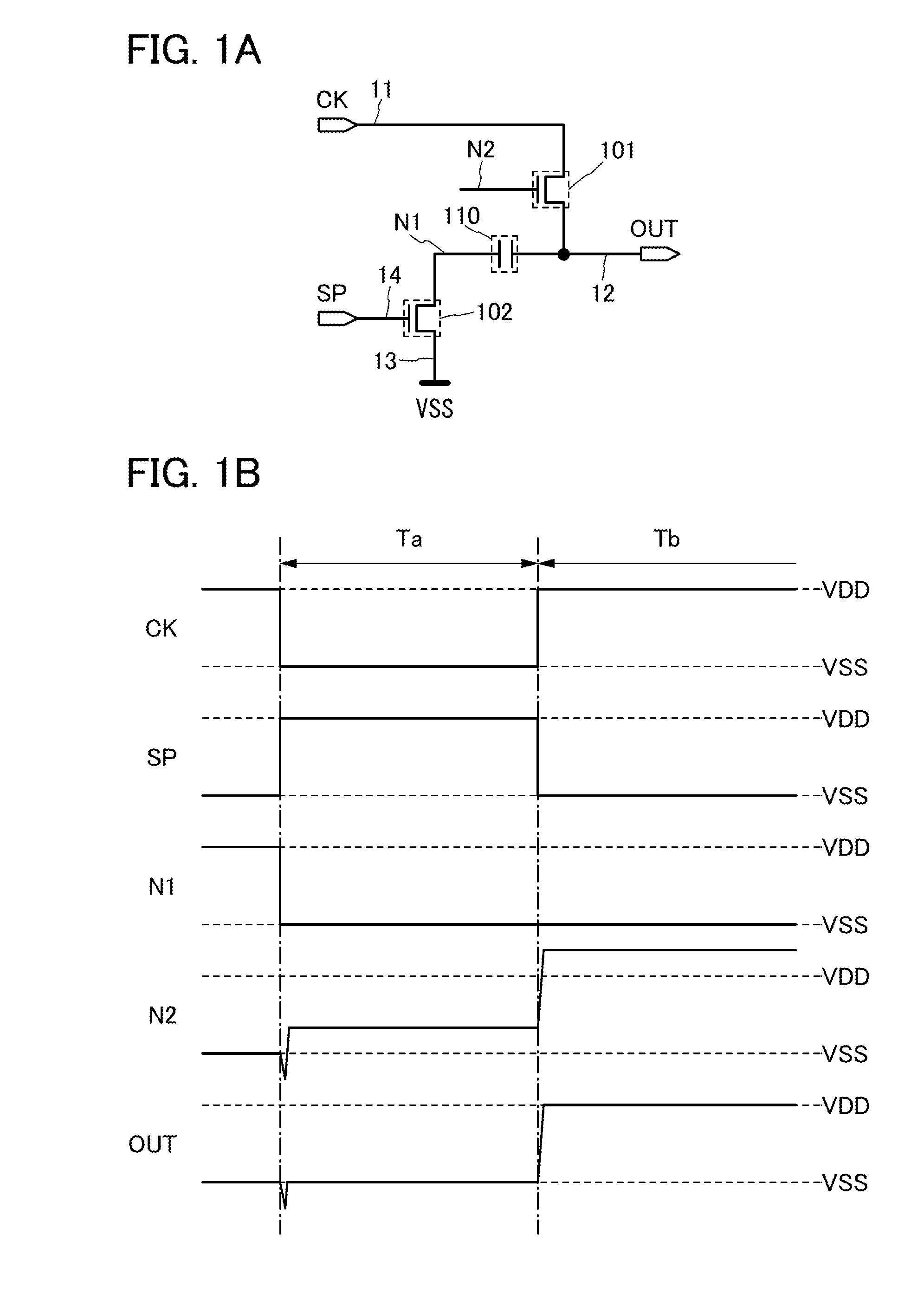
[0042]First, the configuration of a basic circuit in this embodiment will be described with reference to FIG. 1A.
[0043]The basic circuit in FIG. 1A includes a transistor 101, a transistor 102, and a capacitor 110.
[0044]A first terminal of the transistor 101 is connected to a wiring 11. A second terminal of the transistor 101 is connected to a wiring 12.
[0045]A first terminal of the transistor 102 is connected to a wiring 13. A gate of the transistor 102 is connected to a wiring 14.
[0046]A first electrode (also referred to as one electrode) of the capacitor 110 is connected to the wiring 12. A second electrode (also referred to as the other electrode) of the capacitor 110 is connected to a second terminal of the transistor 102.
[0047]Note that the second terminal of th...
embodiment 2
[0122]In this embodiment, a basic circuit including a buffer circuit and a sequential circuit including the basic circuit will be described.
[0123]First, the configuration of a basic circuit in this embodiment will be described with reference to FIG. 6A. The basic circuit in FIG. 6A has a configuration in which a transistor 201 is provided in the basic circuit in FIG. 1A.
[0124]Note that the transistor 201 preferably has the same conductivity type as the transistor 101. In this embodiment, the case where these transistors are n-channel transistors will be described.
[0125]A first terminal of the transistor 201 is connected to the wiring 11. A second terminal of the transistor 201 is connected to a wiring 31. A gate of the transistor 201 is connected to the gate of the transistor 101.
[0126]The transistor 201 has a function of controlling electrical continuity between the wiring 11 and the wiring 31, a function of supplying the signal CK of the wiring 11 to the wiring 31, and a function ...
embodiment 3
[0158]In this embodiment, sequential circuits different from those in Embodiments 1 and 2 will be described.
[0159]A sequential circuit in FIG. 7A has a configuration in which the second terminal of the transistor 105 is connected to the wiring 16 in the sequential circuit in FIG. 3.
[0160]In the sequential circuit in FIG. 7A, the wiring 15 and the potential VDD can be omitted.
[0161]Note that in any of the sequential circuits and the shift register circuit described in Embodiments 1 and 2, the second terminal of the transistor 105 may be connected to the wiring 16.
[0162]A sequential circuit in FIG. 7B has a configuration in which the second terminal of the transistor 105 in the sequential circuit in FIG. 3 is connected to a wiring 17.
[0163]The wiring 17 (also referred to as signal line) is supplied with a signal CKB and has a function of transmitting or supplying the signal CKB. The signal CKB is a signal having high and low levels. The signal CKB corresponds to one of a plurality of ...
PUM
 Abstract
Description
Claims
Application Information
 - R&D
- Intellectual Property
- Life Sciences
- Materials
- Tech Scout
- Unparalleled Data Quality
- Higher Quality Content
- 60% Fewer Hallucinations
Browse by: Latest US Patents, China's latest patents, Technical Efficacy Thesaurus, Application Domain, Technology Topic, Popular Technical Reports.
© 2025 PatSnap. All rights reserved.Legal|Privacy policy|Modern Slavery Act Transparency Statement|Sitemap|About US| Contact US: help@patsnap.com


