
Method for obtaining three-dimensional actin structures and uses thereof

a three-dimensional protein and structure technology, applied in the field of microelectronics, can solve the problems of few studies relating to methods for actually preparing three-dimensional protein structures more complex than nanowires, and the method is quite limited, and the technology is believed to remain inappropriate for the large-scale production of microelectronic devices

Inactive Publication Date: 2015-02-19
COMMISSARIAT A LENERGIE ATOMIQUE ET AUX ENERGIES ALTERNATIVES +1
View PDF12 Cites 1 Cited by
  • Summary
  • Abstract
  • Description
  • Claims
  • Application Information

AI Technical Summary

Benefits of technology

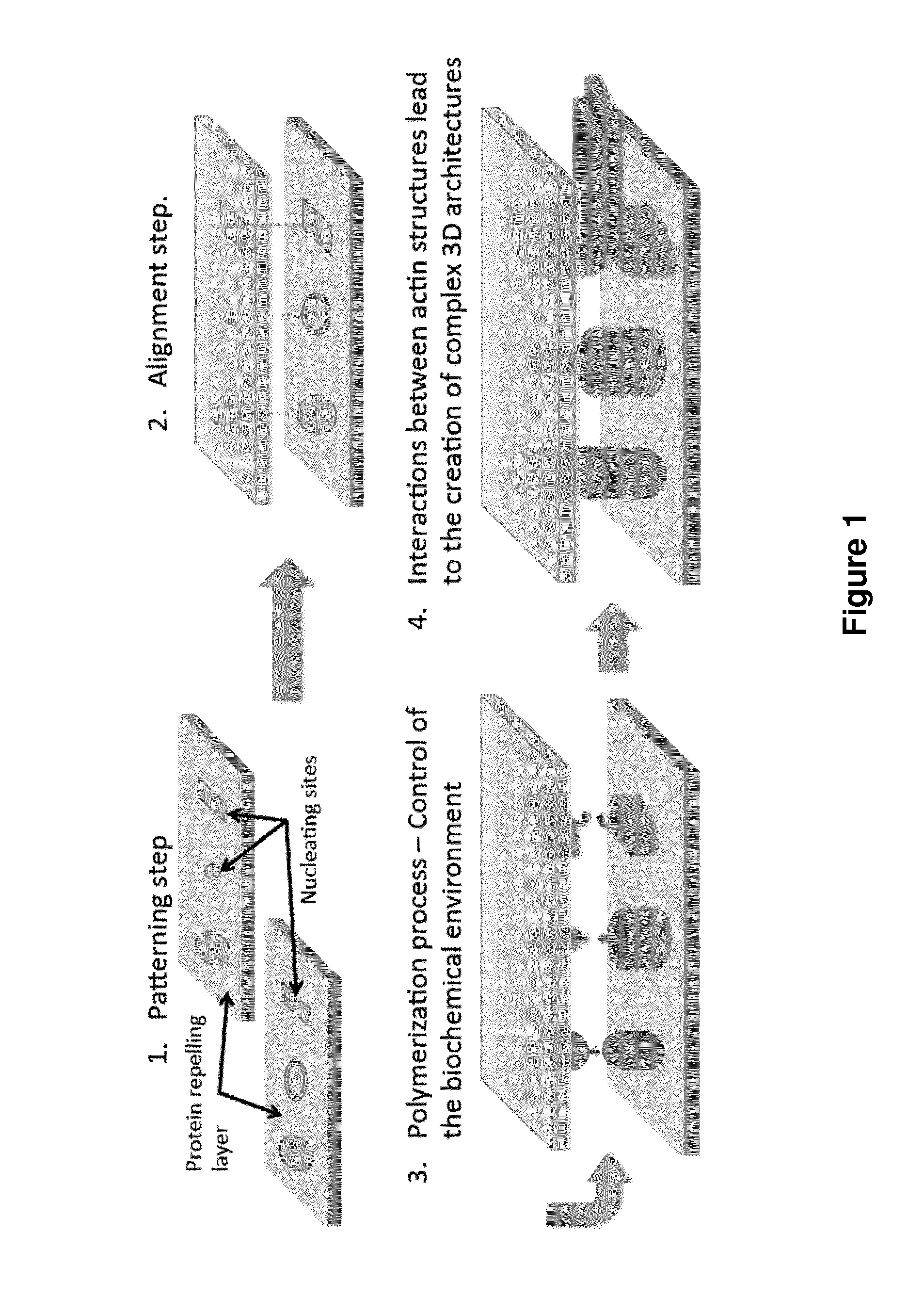
The invention is about a method for creating a three-dimensional actin structure using a polymerization solution containing actin monomers, an Arp2 / 3 complex, a capping agent, a nucleating agent, and a cross-linking protein. The method involves coating a surface with a nucleating agent and then contacting it with a polymerization solution containing actin monomers and an Arp2 / 3 complex. The resulting structure has a unique pattern that can be used to create a conductive connection between two surfaces. The invention also includes a three-dimensional actin structure created using this method.

Problems solved by technology

One of the biggest challenges of 3D-technologies remains the creation of vertical electrical connections between stacked chips or stacked silicon wafers using nano- or microstructures such as nanowires.
But, for the foreseeable future, such technologies are believed to remain inappropriate for the large-scale production of microelectronic devices.
However, few studies relate to methods for actually preparing three-dimensional protein structures more complex than nanowires.
It clearly appears that such a method is quite limited and only enables to obtain very few flat actin structures.
Consequently, the polymerization of actin filaments only occurred from pointed ends and is thus very slow.
Even if the actin filaments grew in out-of-plane direction from the nanopatterns, no well-orientated and well-defined three-dimensional actin structure could be actually observed.
Even if said method virtually enables to control the location of the three-dimensional structures of actin, it clearly appears that such a method is very difficult to implement in mass production process since the distance of the two surfaces must be increased with a very precise rate, during the polymerization process, in order to promote the unidirectional growth of actin filaments.
Moreover, since US 2005 / 0106629 does not provide any experimental result, the experimental feasibility of this method remains to be demonstrated.

Method used


Image

  • Method for obtaining three-dimensional actin structures and uses thereof
  • Method for obtaining three-dimensional actin structures and uses thereof
  • Method for obtaining three-dimensional actin structures and uses thereof

Examples


example 1

“Plug and Receptacle” 3D Connections (See FIGS. 3A and 3B)

[0286]Two clean glass coverslips were made resistant to protein binding by a PLL-PEG treatment. The clean coverslips were first oxidized through oxygen plasma (FEMTO, Diener Electronics, France) 60 s at 30 W. The negatively charged coverslips were then incubated for 30 minutes with a 0.1 mg / mL PLL-PEG (CYTOO, France) diluted in 10 mM HEPES (pH 7.4). The positively charged PLL_PEG molecules were bound to the coverslips through electrostatic interactions creating a protein-repelling layer at their surfaces. After the incubation process, the two glass coverslips were washed with a 1×KMEI buffer to remove the unbound PLL-PEG that is in excess.

[0287]The 1×KMEI buffer is composed of 500 mM KCl, 10 mM MgCl2, 10 mM EGTA and 100 mM imidazole at pH 7 diluted ten times in a G-Actin buffer (2 mM Tris-Cl, 0.2 mM ATP, 0.5 mM DTT, 0.1 mM CaCl2 and 1 mM Na azide).

[0288]The two glass coverslips were then assembled together with one over the o...

example 2

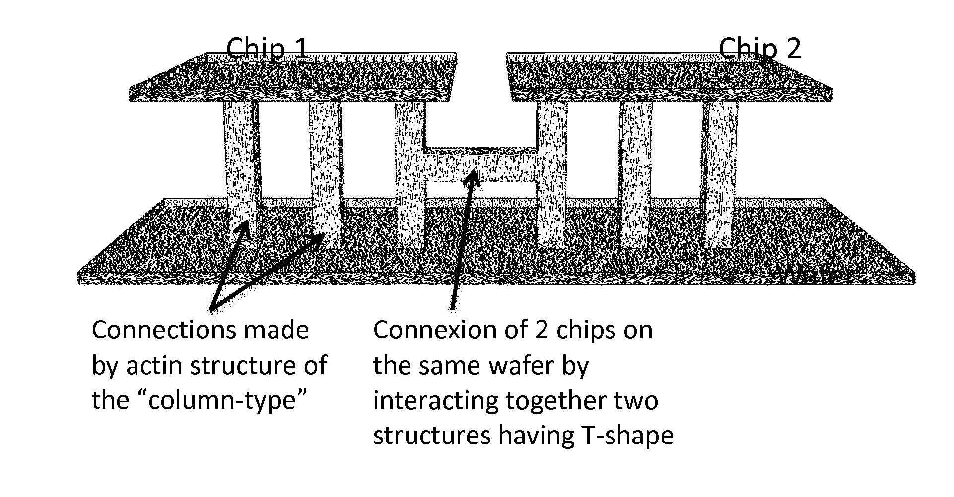
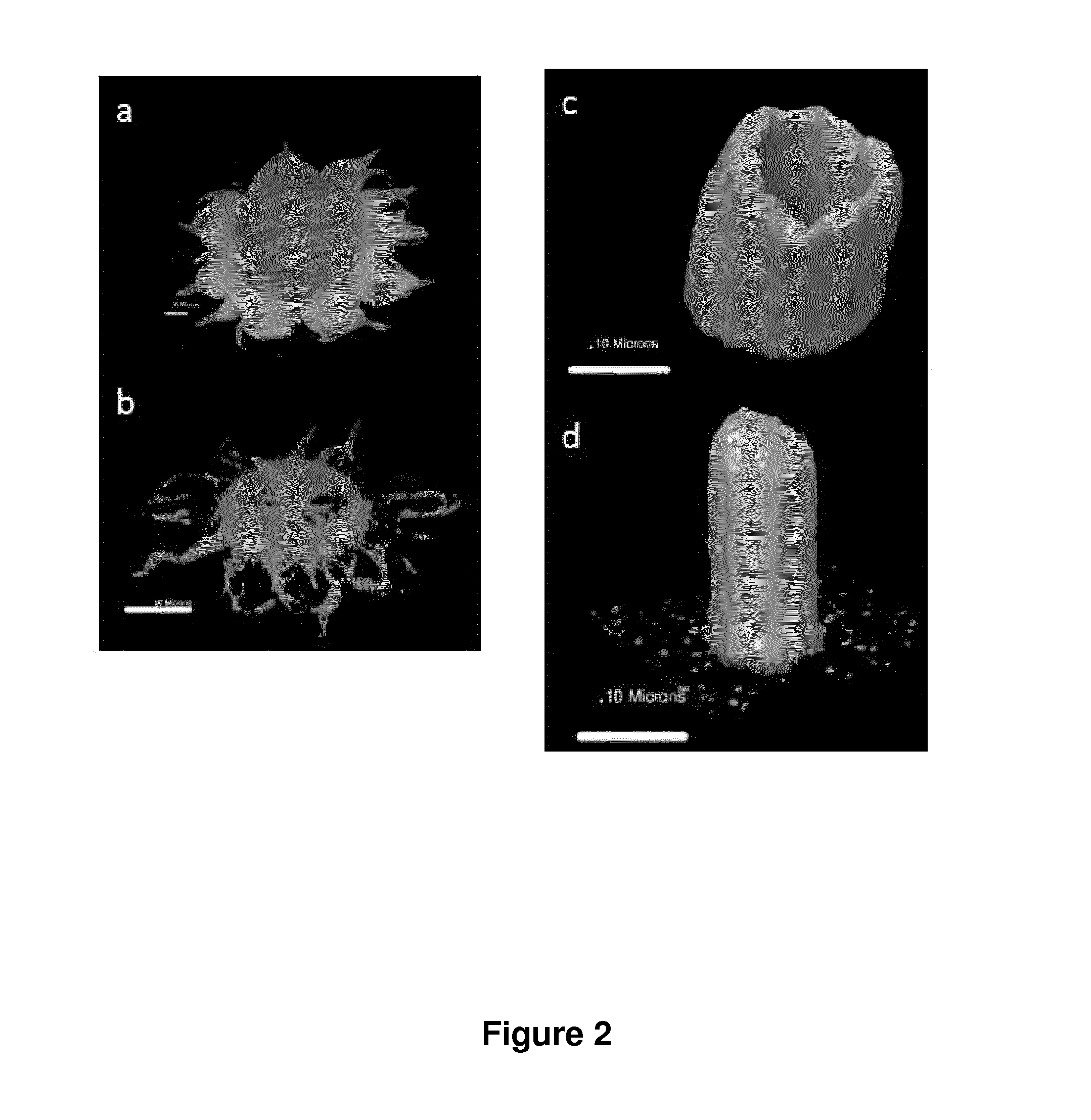
3D Column-Type Structures (FIG. 4)

[0294]Two clean glass coverslips were made resistant to protein binding by a PLL-PEG treatment. The clean coverslips were first oxidized through oxygen plasma (FEMTO, Diener Electronics, France) 60 s at 30 W. The negatively charged coverslips were then incubated for 30 minutes with a 0.1 mg / mL PLL-PEG (CYTOO, France) diluted in 10 mM HEPES (pH 7.4). The positively charged PLL_PEG molecules were bound to the coverslips through electrostatic interactions creating a protein-repelling layer at their surfaces. After the incubation process, the two glass coverslips were washed with a 1×KMEI buffer to remove the unbound PLL-PEG that is in excess. The 1×KMEI buffer was composed of 500 mM KCl, 10 mM MgCl2, 10 mM EGTA and 100 mM imidazole at pH 7 diluted ten times in a G-Actin buffer (2 mM Tris-Cl, 0.2 mM ATP, 0.5 mM DTT, 0.1 mM CaCl2 and 1 mM Na azide).

[0295]The two glass coverslips were then assembled together with one over the other thanks to two double fa...

example 3

Building Blocks Having T-Shape Structure

[0301]Two clean glass coverslips were made resistant to protein binding by a PLL-PEG treatment. The clean coverslips were first oxidized through oxygen plasma (FEMTO, Diener Electronics, France) 60 s at 30 W. The negatively charged coverslips were then incubated for 30 minutes with a 0.1 mg / mL PLL-PEG (CYTOO, France) diluted in 10 mM HEPES (pH 7.4).

[0302]The positively charged PLL_PEG molecules were bound to the coverslips through electrostatic interactions creating a protein-repelling layer at their surfaces. After the incubation process, the two glass coverslips were washed with a 1×KMEI buffer to remove the unbound PLL-PEG that is in excess. The 1×KMEI buffer was composed of 500 mM KCl, 10 mM MgCl2, 10 mM EGTA and 100 mM imidazole at pH 7 diluted ten times in a G-Actin buffer (2 mM Tris-Cl, 0.2 mM ATP, 0.5 mM DTT, 0.1 mM CaCl2 and 1 mM Na azide).

[0303]The two glass coverslips were then assembled together with one over the other thanks to tw...


PUM

PropertyMeasurementUnit
Lengthaaaaaaaaaa
Molar densityaaaaaaaaaa

Abstract

The present invention relates to a method for preparing three-dimensional actin structures having a well-defined shape and displaying improved mechanical rigidity. This method comprises the steps of (a) providing a polymerization solution comprising actin monomers, a branching agent and a capping agent, (b) providing at least one surface having thereon a pattern which is coated with a nucleating agent, and (c) contacting the at least one surface of step (b) with the polymerization solution of step (a) so as to induce the polymerization of actin and obtain the said desired three-dimensional actin structure. Applications of the present invention in various technological fields such as microelectronics are also provided.

Description

FIELD OF THE INVENTION[0001]The present invention relates to a method for preparing oriented three-dimensional actin structures of the nano- or micrometer scale, and uses thereof, in particular, in the fields of microelectronics.BACKGROUND OF THE INVENTION[0002]The development of new methods for preparing three-dimensional structures of the nano- or the micrometre scale is of great interest in various technological fields such as biotechnology, microelectronics, microfluidics and biomaterials.[0003]In microelectronics, research have focused on the development of new approaches for miniaturizing classical 2D integrated circuits into smaller 3D-structures in which interconnected silicon wafers (3D-IC (3D-integrated circuits)) or chips (3D-packaging) are stacked. The so-called “3D-technology” enables to provide greater functionality and higher component density while decreasing the form factor. One of the biggest challenges of 3D-technologies remains the creation of vertical electrical...

Claims


Application Information

Patent Timeline
IPC IPC(8): H01L23/00B29C41/00C07K14/47
CPCH01L24/64C07K14/4716H01L2924/0695H01L24/70B29C41/003B82Y15/00B82Y5/00B82Y40/00B82B3/0052B82B3/0019H01L25/0652H01L25/0657H01L2225/06517H01L2225/06513H01L2225/06524H01L2224/16105H01L2224/16137H01L2224/13693H01L2224/16106H01L2224/16059H01L2224/1366H01L24/11H01L24/13H01L24/16H01L2224/13018H01L2224/13193H01L2224/13639H01L2224/13644H01L2224/13647H01L2224/16145H01L2224/1613H01L25/50H01L2924/1461H01L2924/12042H01L24/82H01L2224/24137H01L2224/245H01L2224/82101H01L2224/11524H01L24/14H01L24/17H01L2224/14051H01L2924/00014H01L2924/00012H01L2924/00
Inventor GABRIEL, JEAN-CHRISTOPHEBLANCHOIN, LAURENTTHERY, MANUELGALLAND, REMI
Owner COMMISSARIAT A LENERGIE ATOMIQUE ET AUX ENERGIES ALTERNATIVES
Learn More