OLED Packaging Structure and Packaging Method
- Summary
- Abstract
- Description
- Claims
- Application Information
AI Technical Summary
Benefits of technology
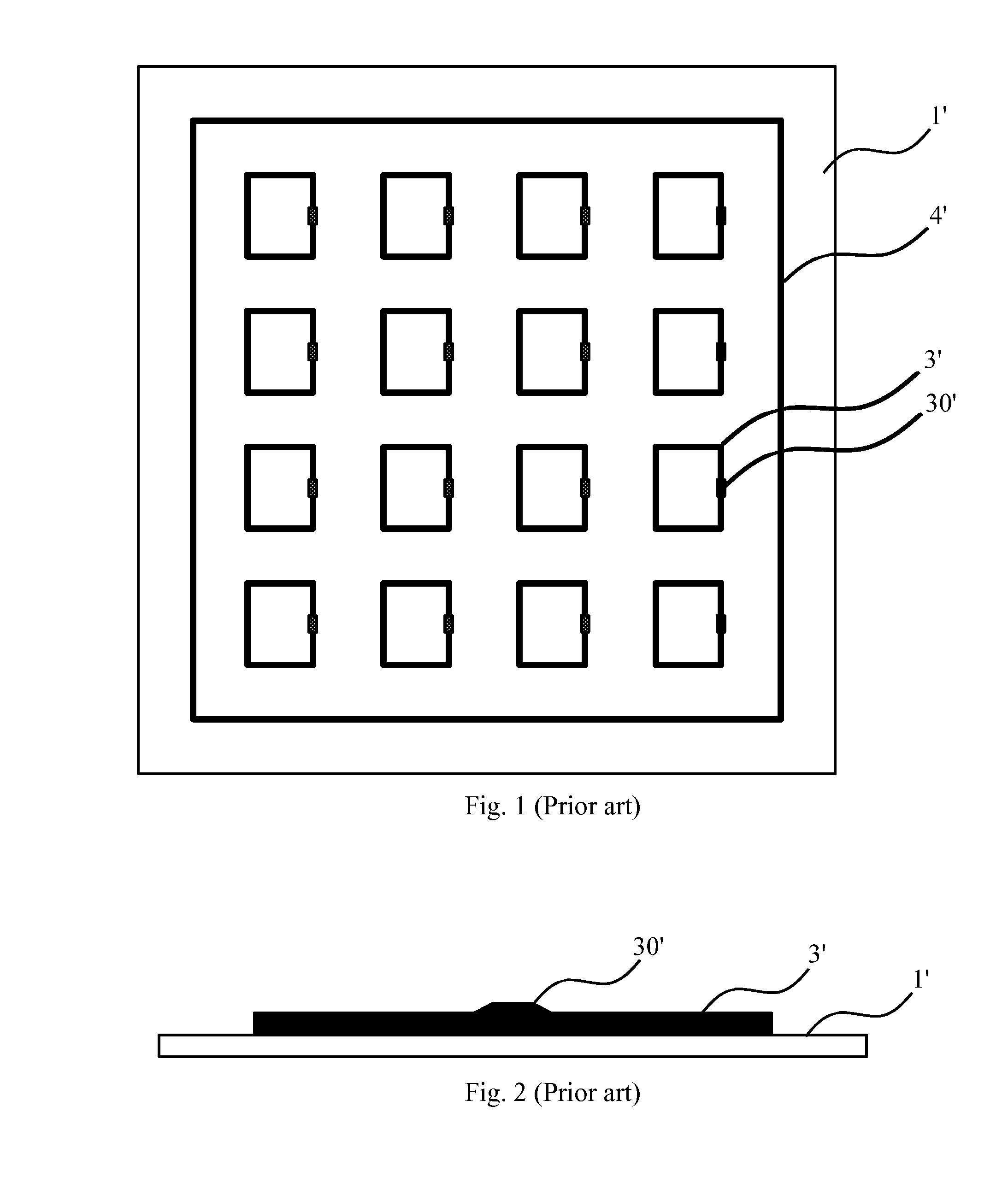
Problems solved by technology
Method used
Image
Examples
first embodiment
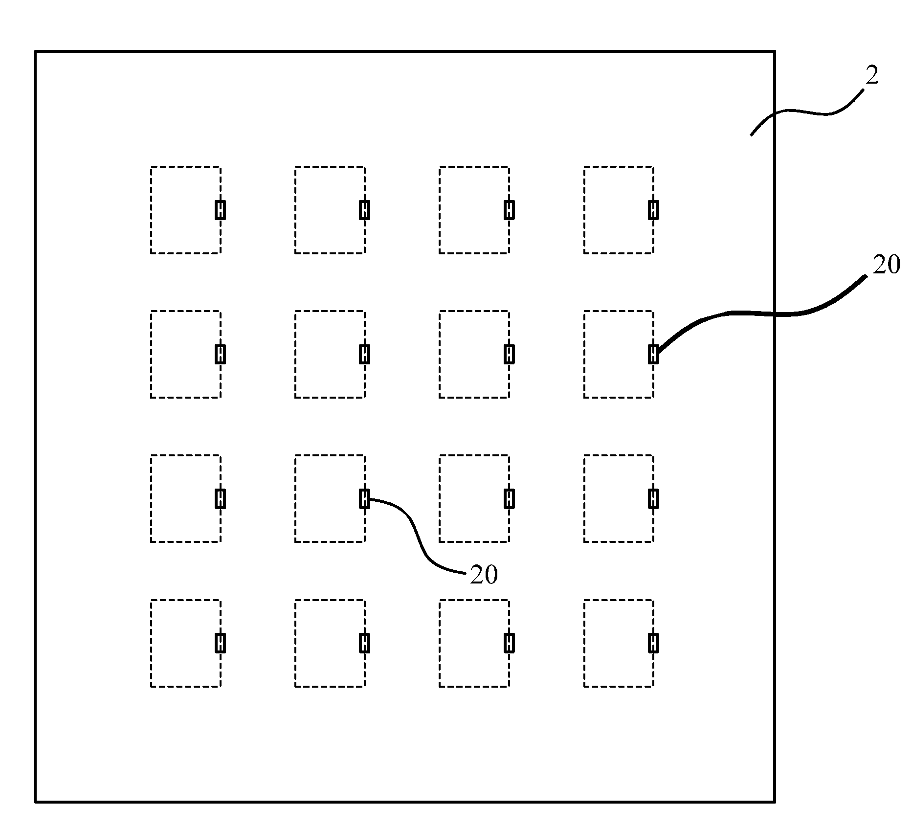
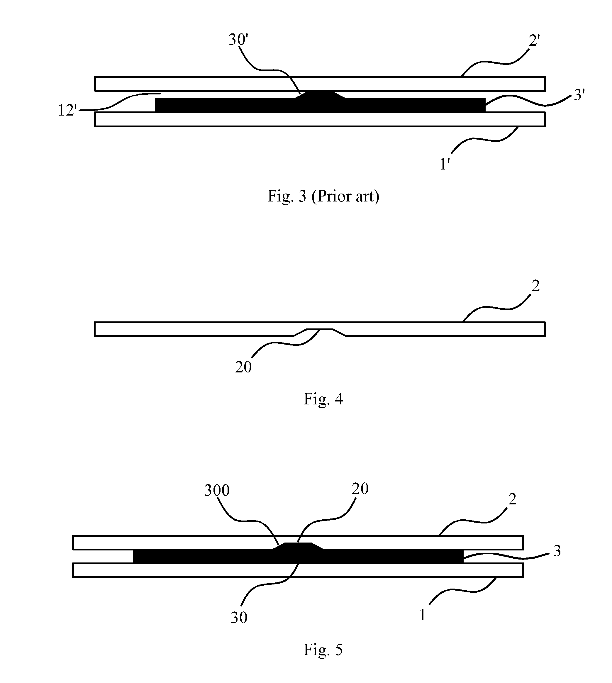
[0030]Please refer to FIG. 4 through FIG. 6, the packaging structure according to the present invention comprises a packaging board 1 and an OLED substrate 2. At least a seal frame 3 is formed by painting glass frit seal on a position of the packaging board 3. A size of the seal frame 3 matches the OLED. An initial painting point 30 is on every seal frame 3. A prominence 300 on the initial painting point 30 protrudes the seal frame 3. A recess 20 is set up on the OLED substrate 2 corresponding to the initial painting point 30 to accommodate the prominence 300.
[0031]Since the prominence 300 on the initial painting point 30 protrudes from the seal frame 3 due to accumulation of glass frit seal on the packaging board 1, the present inventive embodiment improve the OLED substrate 2. Because the OLED substrate 2 is adhesive to the packaging board 1 in pair, the seal frame 3 on the packaging board 1 wards off the OLED on the OLED substrate 2 correspondingly to form a sealed cavity to keep...
second embodiment
[0033]Please refer to FIG. 7. According to the OLED packaging structure, an OLED packaging method provided in the second embodiment comprises:
[0034]Step S1, painting glass frit seal at a position corresponding to the OLED on the packaging board 1 to form at least a seal frame 3 matching the OLED in size and the seal frame 3 comprising a protruding prominence 300 out of the seal frame 3 at the initial painting point 30;
[0035]Step S2, setting up the recess 20 at a position corresponding to the initial painting point 30 on the OLED substrate 2 to accommodate the prominence 300;
[0036]In detail, the recess 20 is formed by acid etching and matches the prominence 300 in size and shape. Cross-sectional views of the recess 20 and the prominence 300 are both trapezoid, and the recess 20 and the OLEDs locate on the same side of the OLED substrate 2.
[0037]Step S3, adhering the OLED substrate 2 to the packaging board 1 in pair and accommodating the prominence 300 in the recess 20; and
[0038]Step ...
PUM
 Abstract
Description
Claims
Application Information
 - Generate Ideas
- Intellectual Property
- Life Sciences
- Materials
- Tech Scout
- Unparalleled Data Quality
- Higher Quality Content
- 60% Fewer Hallucinations
Browse by: Latest US Patents, China's latest patents, Technical Efficacy Thesaurus, Application Domain, Technology Topic, Popular Technical Reports.
© 2025 PatSnap. All rights reserved.Legal|Privacy policy|Modern Slavery Act Transparency Statement|Sitemap|About US| Contact US: help@patsnap.com


