
Substrate etching method and substrate processing device

a substrate and processing device technology, applied in the field of microelectronics technology, can solve the problems of difficult control of sidewall morphology, unsatisfactory product result of such an etching, and uneven sidewall of etched section, so as to increase the process quality of substrate, stable state rapidly, and increase the effect of process performan

Active Publication Date: 2014-12-11
BEIJING NAURA MICROELECTRONICS EQUIP CO LTD
View PDF5 Cites 2 Cited by
  • Summary
  • Abstract
  • Description
  • Claims
  • Application Information

AI Technical Summary

Benefits of technology

The substrate etching method and substrate processing device provided by this patent invention allow for a single etching operation mode and a combined operation mode, in which etching and deposition operations are performed simultaneously. This results in smoother etched substrates and higher process quality. The method also allows for easy adjustment of process parameters and an increase in process performance. Additionally, the invention allows for synchronous adjustment of different process parameters, saving time and increasing efficiency of the process.

Problems solved by technology

In practical application, since the etching procedure is isotropic etching, it is difficult to control sidewall morphology.
The defects in the prior art are: since the etching operation and the deposition operation are performed alternately, the polymer deposited on the sidewall of the etched section is not smooth, and so the product resulted from such an etching is not ideal.

Method used


Image

  • Substrate etching method and substrate processing device
  • Substrate etching method and substrate processing device
  • Substrate etching method and substrate processing device

Examples


Embodiment Construction

[0034]The following will describe embodiments of the invention in detail and examples of the embodiments are illustrated in the accompanying drawings, wherein like or similar reference numerals indicate like or similar elements or elements with like or similar functions throughout the description. The embodiments described below referring to the drawings are exemplary, are only used to explain the invention and are not intended to limit the invention.

[0035]The following disclosure provides various embodiments or examples to implement various structures of the invention. In order to simply the disclosure, components and configurations of specific examples will be described in the following. Of course, they are merely examples and are not intended to limit the invention. In addition, the invention may refer to numbers and / or letters repeatedly in different examples. Such a repetition is intended to simplify and clarify, and does not indicate relationship between the discussed various ...


PUM

PropertyMeasurementUnit
etching depthaaaaaaaaaa
excitation poweraaaaaaaaaa
bias poweraaaaaaaaaa

Abstract

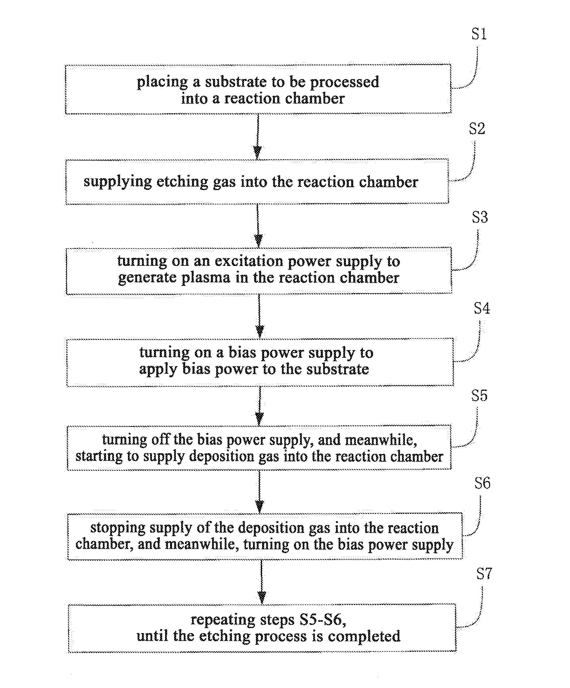
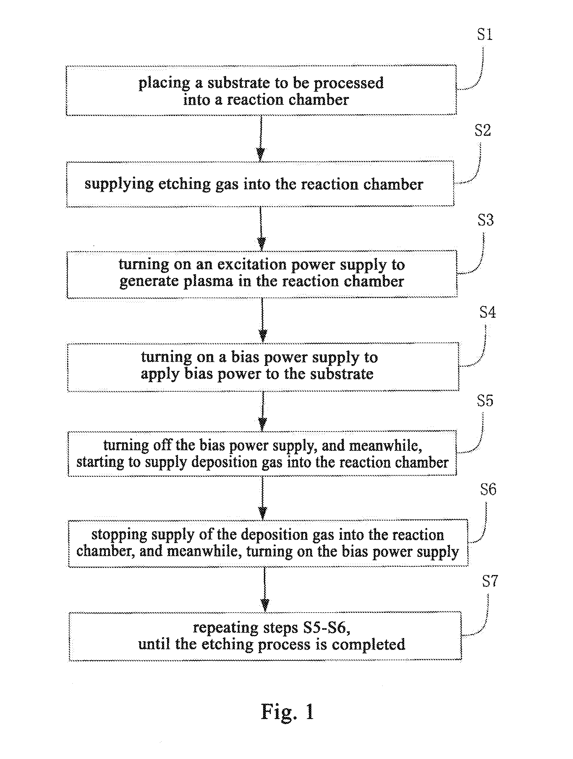
A substrate etching method and a substrate processing device, the substrate etching method includes: S1: placing a substrate to be processed into a reaction chamber; S2: supplying etching gas into the reaction chamber; S3: turning on an excitation power supply to generate plasma in the reaction chamber; S4: turning on a bias power supply to apply bias power to the substrate; S5: turning off the bias power supply, and meanwhile, starting to supply deposition gas into the reaction chamber; S6: stopping supply of the deposition gas into the reaction chamber, and meanwhile, turning on the bias power supply; S7: repeating steps S5-S6, until the etching process is completed. In the whole etching process, the etching operation is always performed, and the deposition operation is performed sometimes. Therefore, during the deposition operation, the plasma in the reaction chamber can etch away at least a part of deposited polymers formed by the deposition operation on a sidewall of an etched section, so that the sidewall of the etched section of the substrate is smooth.

Description

FIELD OF THE INVENTION[0001]The present invention relates to the field of microelectronics technology, and particularly relates to a substrate etching method and a substrate processing device.BACKGROUND OF THE INVENTION[0002]As MEMS devices and MEMS systems are widely used in the field of automobile and consumer electronics, and through-silicon via (TSV) etch technology has wide prospect in the field of packaging, plasma deep silicon dry etching process gradually becomes one of the most important processes in the field of MEMS manufacturing and TSV technology.[0003]Deep silicon etching process is different from a general silicon etching process in that: etching depth of the deep silicon etching process is much larger than that of the general silicon etching process and is generally several tens of micrometers or even up to one hundred meters, and however etching depth of the general silicon etching process is smaller than 1 micrometer. In order to etch a silicon material of several ...

Claims


Application Information

Patent Timeline
Patent Type & Authority Applications(United States)
IPC IPC(8): B81C1/00B81C99/00
CPCB81C99/0025B81C1/00531H01L21/30655B81C1/00619B81C2201/0132
Inventor WEI, GANGWANG, CHUNLI, DONGSAN
Owner BEIJING NAURA MICROELECTRONICS EQUIP CO LTD
Learn More