
Touch sensing apparatus using touch pattern without insulation and method for manufacturing the same

a touch sensor and pattern technology, applied in the direction of conductive pattern formation, instruments, optics, etc., can solve the problems of high error rate, difficult to determine the self-capacitance type touch input, and the mutual-capacitance touch sensing apparatus requires a more complex process, and achieves a simple multi-layer structure and low manufacturing cost.

Inactive Publication Date: 2014-11-20
MELFAS
View PDF3 Cites 9 Cited by
  • Summary
  • Abstract
  • Description
  • Claims
  • Application Information

AI Technical Summary

Benefits of technology

This patent text describes a touch location sensing panel that has low manufacturing costs and is easy to produce. It also describes how the panel uses a limited number of channels in the touch sensing circuit, which helps save money and improve productivity. This results in a more efficient and economical touch panel.

Problems solved by technology

However, it is not easy for the self-capacitance type to determine a touch input.
As a result, when manufacturing an external wire region of the touch sensing device, the mutual-capacitance touch sensing apparatus requires a more complex process and there is a disadvantage of a high error rate, compared with a conventional external wire region manufacturing method.

Method used


Image

  • Touch sensing apparatus using touch pattern without insulation and method for manufacturing the same
  • Touch sensing apparatus using touch pattern without insulation and method for manufacturing the same
  • Touch sensing apparatus using touch pattern without insulation and method for manufacturing the same

Examples


Embodiment Construction

[0052]Exemplary embodiments of the disclosed subject matter are described more fully hereinafter with reference to the accompanying drawings. The disclosed subject matter may, however, be embodied in many different forms and should not be construed as limited to the exemplary embodiments set forth herein. Rather, the exemplary embodiments are provided so that this disclosure is thorough and complete, and will convey the scope of the disclosed subject matter to those skilled in the art. In the drawings, the size and relative sizes of layers and regions may be exaggerated for clarity. Like reference numerals in the drawings denote like elements.

[0053]It will be understood that when an element or layer is referred to as being “on”, “connected to”, or “coupled to” another element or layer, it can be directly on, connected, or coupled to the other element or layer or intervening elements or layers may be present. In contrast, when an element is referred to as being “directly on”, “direct...


PUM

PropertyMeasurementUnit
dielectric constantaaaaaaaaaa
thicknessaaaaaaaaaa
temperatureaaaaaaaaaa

Abstract

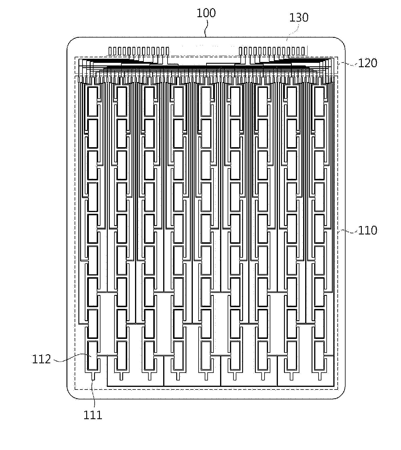
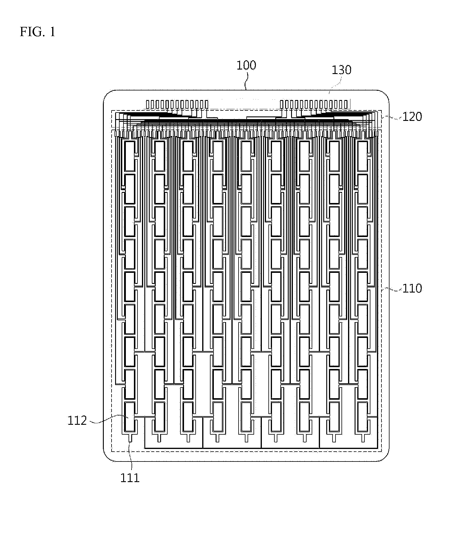
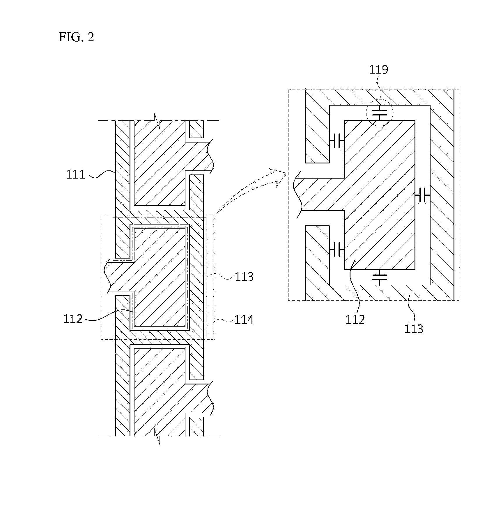
A touch location sensing panel includes a touch detection region in which a plurality of sensing regions are arranged on a single substrate in two columns, an external wire region provided in one outer side surface of the touch detection region, a plurality of transmitting (Tx) electrodes formed in the plurality of the sensing regions, with at least one patch shape, respectively, to sense a location of touch applied to the touch detection region on a second axis, a plurality of receiving (Rx) electrodes electrically separated from the transmitting electrodes in the plurality of the sensing regions and extended along a second axis to cover the transmitting electrodes, to sense a location of the touch on a first axis, and a plurality of internal wires arranged in the same layer with the plurality of the transmitting electrodes and the plurality of the receiving electrodes, and connected to plurality of the transmitting electrodes and the plurality of the receiving electrodes to be extended to the external wire region.

Description

[0001]This application claims priority from and the benefit of Korean Patent Application No. 10-2013-0054951, filed on May 15, 2013, which is hereby incorporated by reference for all purposes as if fully set forth herein.BACKGROUND OF THE DISCLOSURE[0002]1. Field of the Disclosure[0003]Exemplary embodiments of the disclosure relate to a touch sensing apparatus using a touch pattern without insulation and a method for manufacturing the same.[0004]2. Discussion of the Background[0005]A touch sensing apparatus is one of input devices configurating interfaces between a user and an information communication device using various displays. Such a touch sensing apparatus helps a user to directly touch a screen, using an input tool such as his or her hand or a pen, to make it easy to implement inputs more easily.[0006]The touch sensing apparatus may be classified into a resistive type, a capacitive overlay type, an ultrasonic type and an infrared type. The capacitive type touch sensing appar...

Claims


Application Information

Patent Timeline
Patent Type & Authority Applications(United States)
IPC IPC(8): G06F3/044
CPCG06F3/044G06F2203/04103G06F2203/04107G06F2203/04112Y10T29/49155G06F3/0443G06F3/0446
Inventor KIM, KWANG HYUN
Owner MELFAS
Learn More