
Electric current application method and electric current applying device

Active Publication Date: 2014-11-13
HONDA MOTOR CO LTD
View PDF6 Cites 1 Cited by
  • Summary
  • Abstract
  • Description
  • Claims
  • Application Information

AI Technical Summary

Benefits of technology

The present invention provides an electric current application method and device that prevents damage to a semiconductor caused by residual electricity. The method involves eliminating residual electricity from the first electric current carrying part and the second electric current carrying part by making the first electrode contact the first electric current carrying part in a residual electricity eliminating step prior to the second electrode contacting the second electric current carrying part in the main electric current conducting step. This prevents electrical voltage from arising between the gate-emitter, which are at locations of the lowest withstand voltage in the semiconductor, and thus prevents damage of the semiconductor caused by residual electricity. The residual electricity is ultimately eliminated from the semiconductor after electric current application. Overall, this invention provides a safer and more reliable method of applying electric current to semiconductors.

Problems solved by technology

In this regard, when residual electricity in the semiconductor is transmitted to the probe pin the instant when making the probe pin contact with the semiconductor, an electrical voltage exceeding the withstand voltage occurs between the gate-emitter, which is the site of lowest withstand voltage in the semiconductor, and the semiconductor may be destroyed.

Method used


Image

  • Electric current application method and electric current applying device
  • Electric current application method and electric current applying device
  • Electric current application method and electric current applying device

Examples


Embodiment Construction

[0027]Hereinafter, an embodiment of the present invention will be explained.

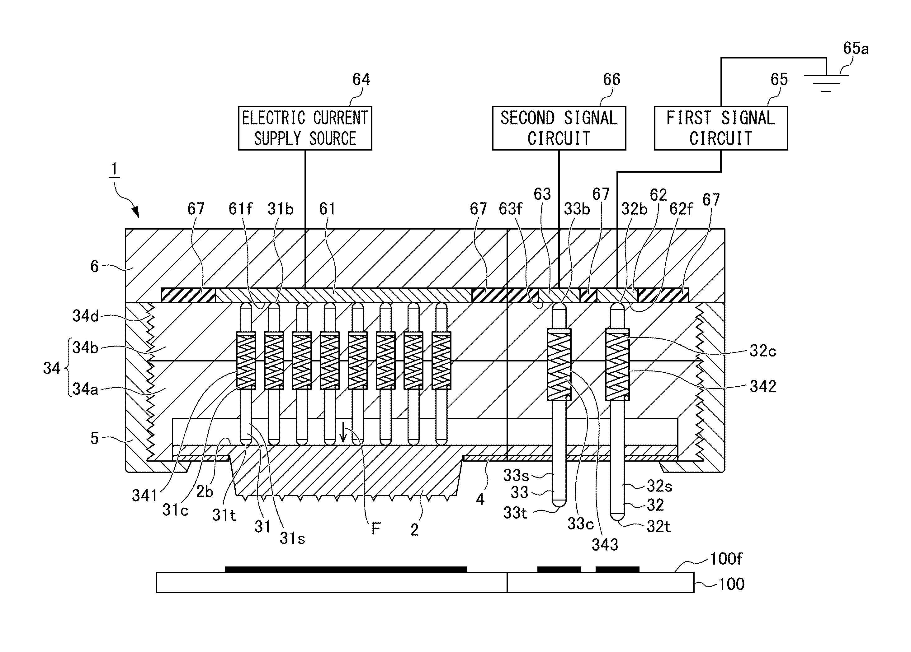
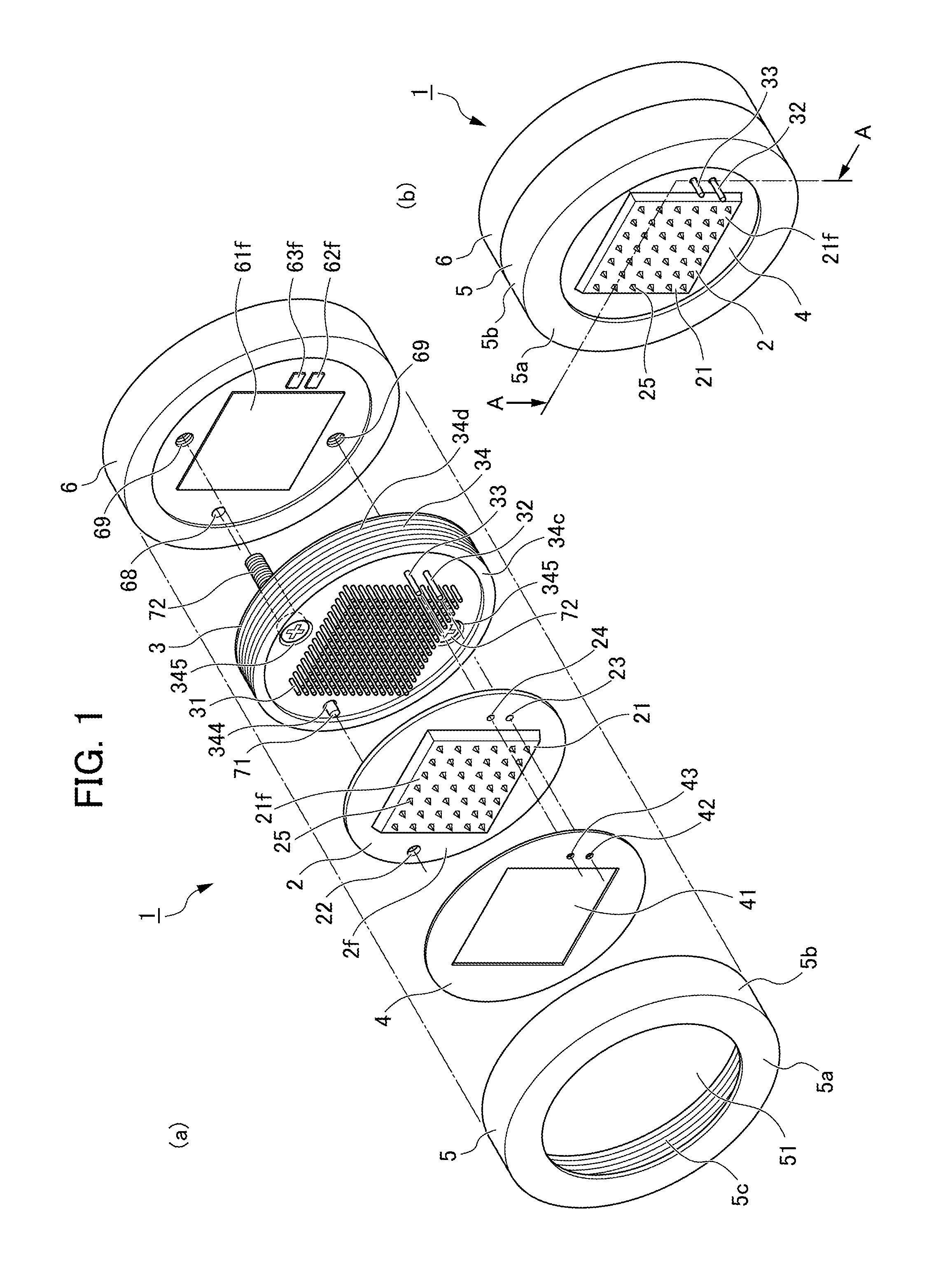
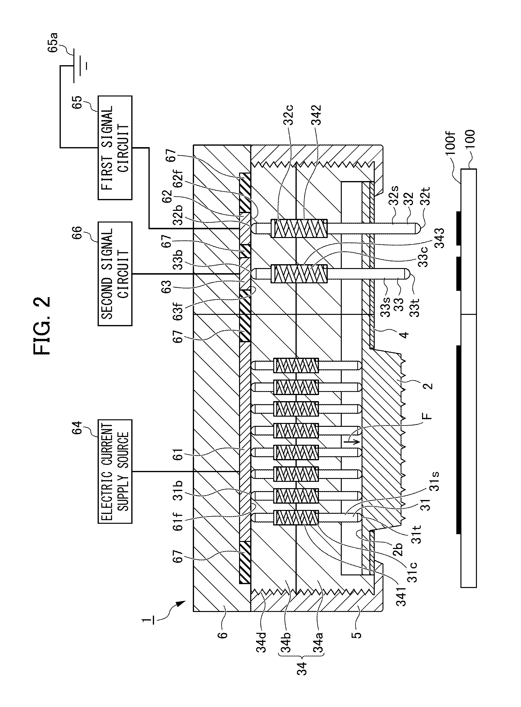
[0028]FIG. 1 provides perspective views showing an outline configuration of a probe device 1 as a electric current applying device according to an embodiment of the present invention, with FIG. 1(a) being an exploded view and FIG. 1(b) being an overall view. FIG. 2 is a cross-sectional view along the line AA in FIG. 1(b) of the probe device 1 according to the embodiment. The cross-section along the line AA in FIG. 1(b) changes the cross-sectional position midway in order to facilitate understanding of the cross-sectional configuration of the probe device 1.

[0029]The probe device 1 shown in FIG. 1 is applied to a semiconductor inspection device for inspecting a power semiconductor (IGBT, MOS, diodes, etc.) 100 used in the switching of high current of 400 to 2000 A, and applies high current by pressure contacting the power semiconductor 100.

[0030]The probe device 1 includes a contacting body 2, a pressing body...


PUM


Abstract

An electric current application method for applying electric current to a power semiconductor 100 having a first signal pin contact region 102 that conducts a first electric current, and a contacting body contact region 101 that electrically connects with the first signal pin contact region 102 and conducts a second electric current, includes a Step S1 of contacting a first signal pin 32 of a probe device 1 to the first signal pin contact region 102 so as to eliminate residual electricity remaining in the first signal pin contact region 102 and contacting body contact region 101; and Steps S3 and S4 of contacting a contacting part 21 of the contacting body 2 of the probe device 1 to the contacting body contact region 101, and conducting the first electric current and second electric current, after Step S1.

Description

[0001]This application is based on and claims the benefit of priority from Japanese Patent Application No. 2013-098603, filed on 8 May 2013, the content of which is incorporated herein by reference.BACKGROUND OF THE INVENTION[0002]1. Field of the Invention[0003]The present invention relates to an electric current application method and electric current applying device for applying electric current to a semiconductor. In particular, it relates to an electric current application method and electric current applying device used in the inspection of a power semiconductor for which it is necessary to applying high current.[0004]2. Related Art[0005]Heretofore, a technology related to probe pins for high current that makes the leading end of a probe head contact a semiconductor to pass current therethrough has been known (for example, refer to Patent Document 1). With the technology disclosed in Patent Document 1, the probe pin includes: an abutting member in which a plurality of contactin...

Claims


Application Information

Patent Timeline
IPC IPC(8): G01R31/26
CPCG01R31/2601
Inventor AKAHORI, SHIGETOKAMBARA, NOBUO
Owner HONDA MOTOR CO LTD
Learn More