Semiconductor device

a semiconductor and device technology, applied in semiconductor devices, diodes, electrical devices, etc., can solve the problems of large number of defects, and large number of defects near the boundary between the semiconductor substrate and the semiconductor substrate, so as to prevent the degradation of the temperature detection accuracy of the temperature sensing diode part, the effect of significantly reducing the life of the minority carrier

Active Publication Date: 2014-10-30
TOYOTA JIDOSHA KK +1
View PDF4 Cites 32 Cited by
  • Summary
  • Abstract
  • Description
  • Claims
  • Application Information

AI Technical Summary

Benefits of technology

[0010]In the semiconductor device stated above, the isolation trench is formed in the semiconductor substrate. Therefore, a large number of defects are generated near a boundary between the semiconductor substrate and the isolation trench (in short, on the side walls and a bottom wall of the isolation trench). The isolation trench surrounds the outer periphery of the temperature sensing diode part, and passes through the first base region, and the other side wall of the isolation trench is in contact with the temperature sensing diode part. Thus, a large number of defects are generated near a boundary between the first base region and the isolation trench. Therefore, a minority carrier flown into the first base region is captured by the defects, and a lifetime of the minority carrier is significantly reduced compared to a case where the isolation trench is not formed. Hence, even if voltage in a forward direction is applied between the first semiconductor region and the second semiconductor region of the temperature sensing diode part, a current amplification factor hFE of a parasitic bipolar transistor, which is structured by the second conductivity type second semiconductor region, the first conductivity type base region, and the second conductivity type first drift region, becomes an extremely small value. Thus, current flown into the second semiconductor region becomes extremely small. With this structure, in the semiconductor device, in which the temperature sensing diode part and the power semiconductor element part are provided in the same semiconductor substrate, it is possible to prevent degradation of temperature detection accuracy of the temperature sensing diode part.

Problems solved by technology

Therefore, a large number of defects are generated near a boundary between the semiconductor substrate and the isolation trench (in short, on the side walls and a bottom wall of the isolation trench).
Thus, a large number of defects are generated near a boundary between the first base region and the isolation trench.
Thus, current flown into the second semiconductor region becomes extremely small.

Method used


Image

  • Semiconductor device
  • Semiconductor device
  • Semiconductor device

Examples


Embodiment Construction

[0019]Listed are main features of examples explained below. Technical elements stated below are independent from each other, and exert technical usefulness alone or as various combinations, so the technical elements are not limited to combinations stated in claims at the time of filing.

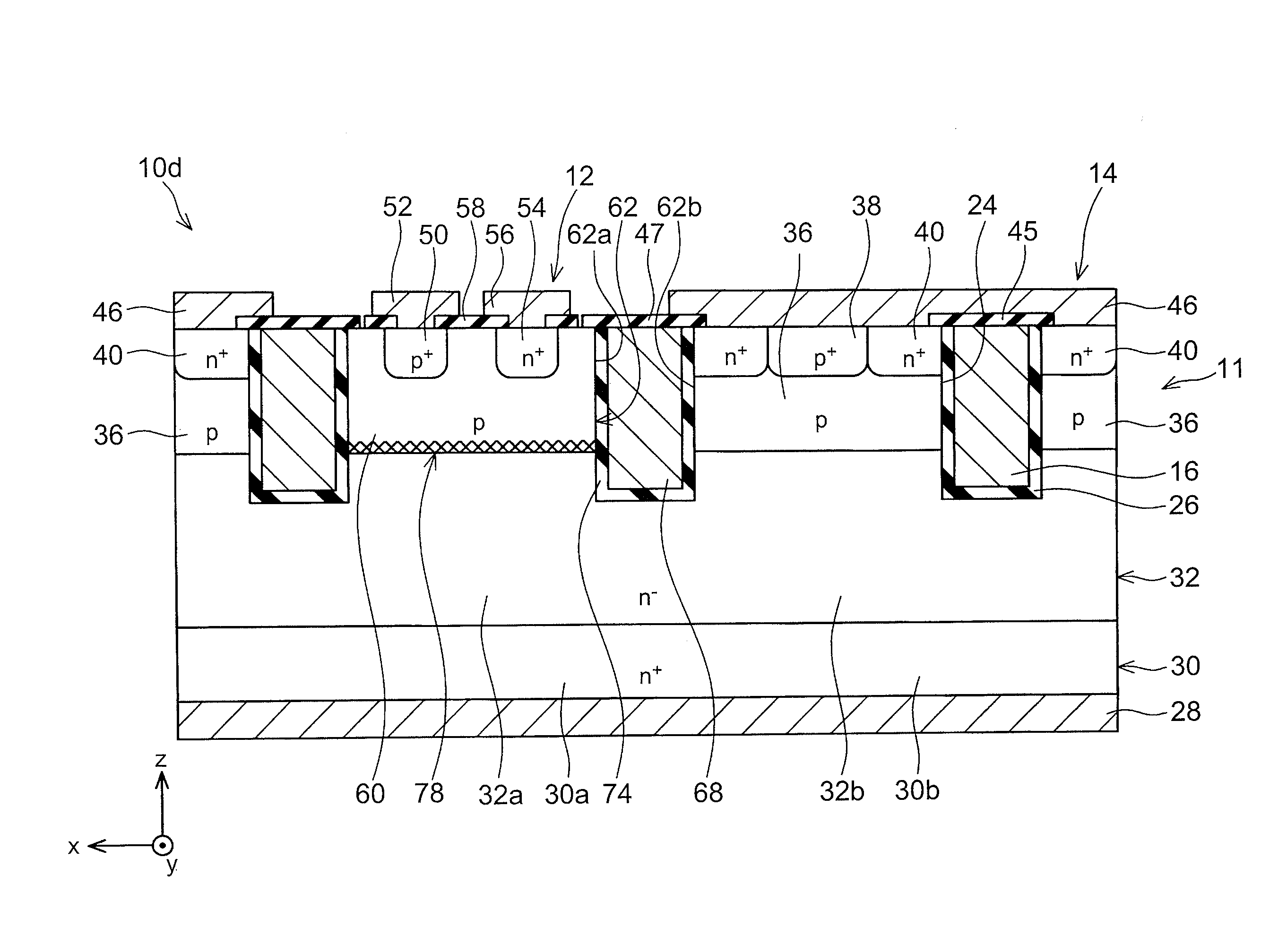
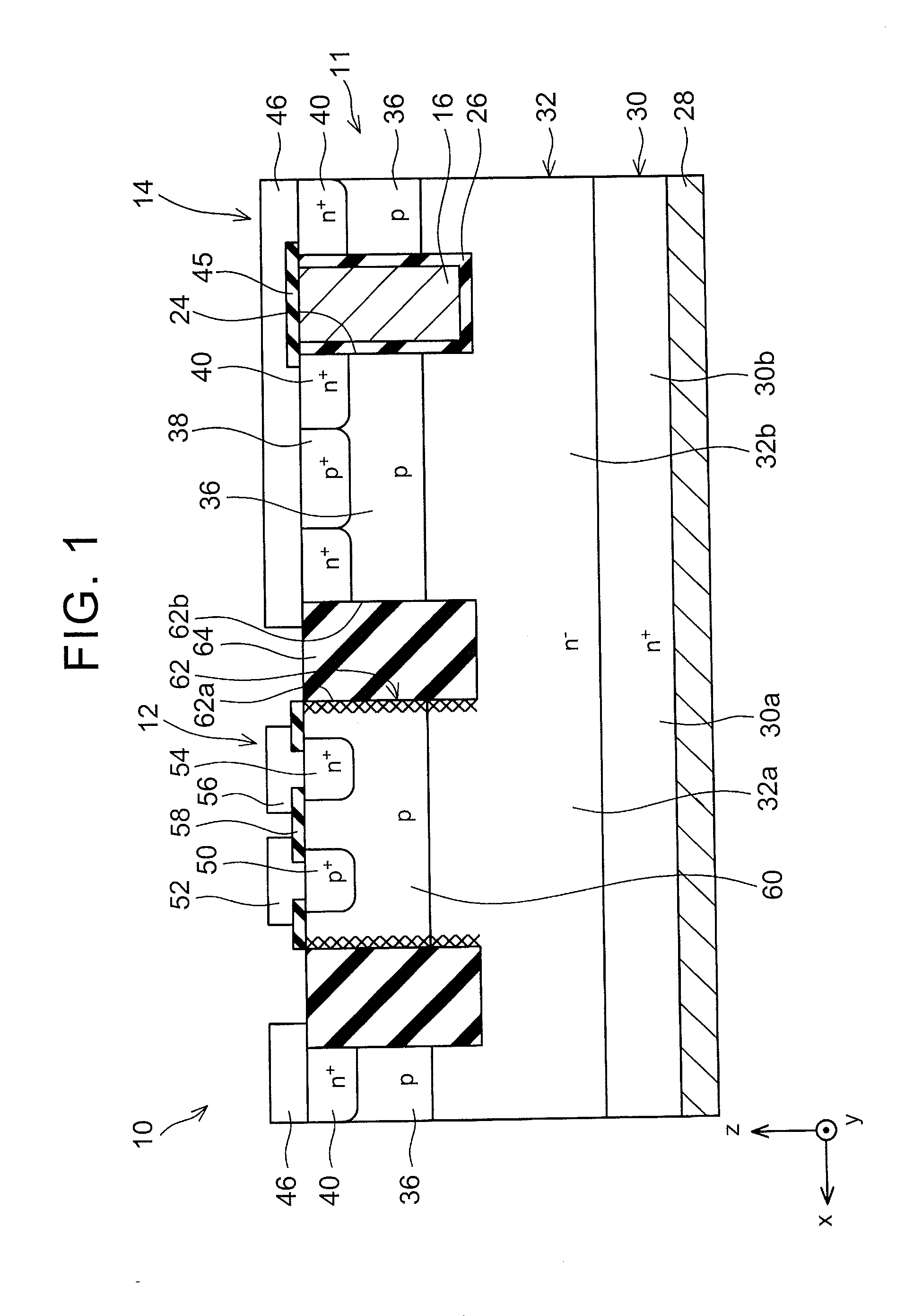
[0020](Feature 1) In a semiconductor device disclosed in this description, an inside of an isolation trench may be entirely filled with an insulator. In general, if an insulator is arranged inside a trench, defects are generated when, for example, the trench is formed, and the defects are generated near regions of side walls and a bottom wall (hereinafter, sometimes simply referred to as “side walls and so on”) of the trench, where the insulator is arranged. When a thickness of the insulator is relatively small, defects are reduced by nitriding. In the above-mentioned semiconductor device, inside of the isolation trench is entirely filled with the insulator. Therefore, the thickness of the insulator b...


PUM


Abstract

A semiconductor device is provided with a semiconductor substrate in which a power semiconductor element part and a temperature sensing diode part are provided. The temperature sensing diode part includes a first semiconductor region, a second semiconductor region, a first base region, and a first drift region. In the semiconductor substrate, an isolation trench is formed, which passes through the first base region, extends to the first drift region, and surrounds an outer periphery of the temperature sensing diode part. At least a part of one of side walls of the isolation trench is in contact with the power semiconductor element part, and the other side wall of the isolation trench is in contact with the temperature sensing diode part.

Description

INCORPORATION BY REFERENCE[0001]The disclosure of Japanese Patent Application No. 2013-092255 filed on Apr. 25, 2013 including the specification, drawings and abstract is incorporated herein by reference in its entirety.BACKGROUND OF THE INVENTION[0002]1. Field of the Invention[0003]A technology disclosed in this description relates to a semiconductor device.[0004]2. Description of Related Art[0005]Japanese Patent Application Publication No. 2012-195339 A (JP 2012-195339 A) discloses a semiconductor device in which a temperature sensing diode and an IGBT are provided in a same semiconductor substrate. It is stated that, in this semiconductor device, it is possible to carry out highly accurate temperature detection in an entire temperature range of rated temperature of the semiconductor device.[0006]In a case where a temperature sensing diode is provided in a semiconductor device, it is normal that a polysilicon layer is formed on an upper surface of a substrate through an insulating...

Claims


Application Information

Patent Timeline
Patent Type & Authority Applications(United States)
IPC IPC(8): H01L27/16
CPCH01L27/16H01L29/0653H01L29/0623H01L29/0696H01L29/1608H01L29/32H01L29/407H01L29/42368H01L29/66068H01L29/7397H01L29/7804
Inventor SUGIMOTO, MASAHIRO
Owner TOYOTA JIDOSHA KK
Why Eureka
Try Eureka