
Effective Caching for Demand-based Flash Translation Layers in Large-Scale Flash Memory Storage Systems

a technology of large-scale flash memory storage and translation layers, applied in the direction of memory adressing/allocation/relocation, instruments, computing, etc., can solve the problems of increasing the capacity of nand flash memory, increasing the difficulty of page-level mapping tables, and occupying a lot of space in the flash memory for dftl

Inactive Publication Date: 2014-10-09
THE HONG KONG POLYTECHNIC UNIV
View PDF3 Cites 32 Cited by
  • Summary
  • Abstract
  • Description
  • Claims
  • Application Information

AI Technical Summary

Benefits of technology

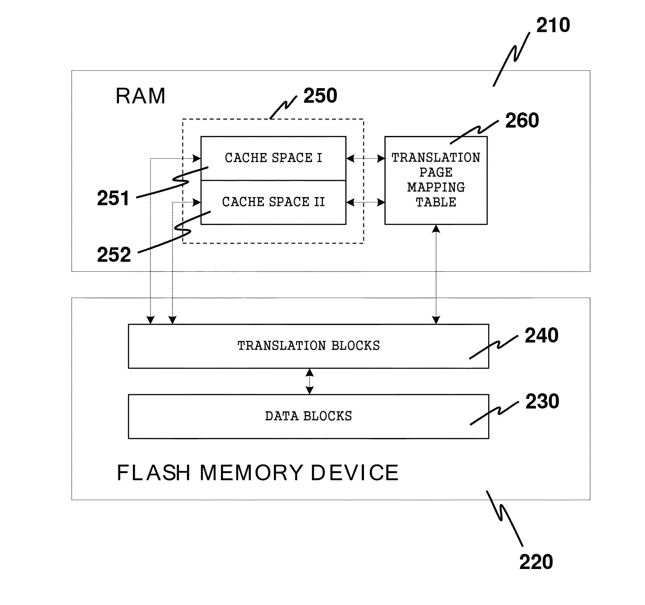
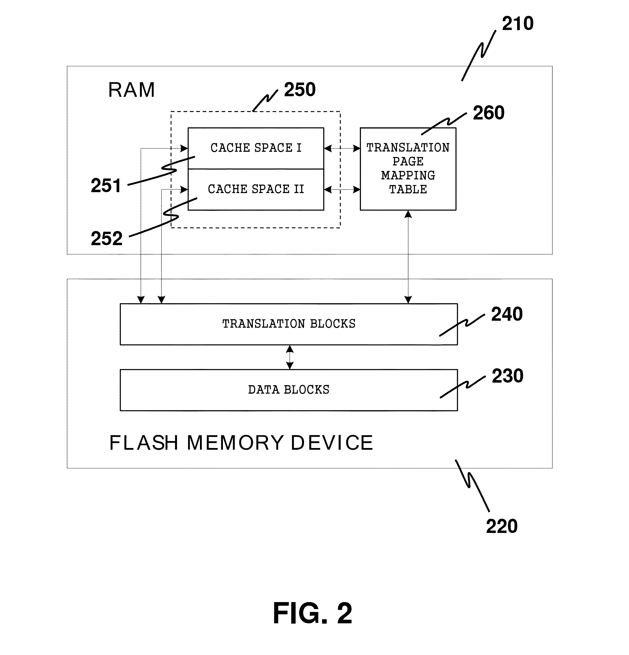
[0019]In particular, the address-translating process is characterized as follows. The DBMTC is searched for identifying, if any, a first-identified data structure selected from among the second address-mapping data structures where the logical block address in the first-identified data structure matches the requested virtual data block address. If the first-identified data structure is identified, the physical block address in the first-identified data structure is assigned as the physical block address corresponding to the requested virtual data block address. If the first-identified data structure is not identified, the TPMT is searched for identifying a second-identified data structure among the third address-mapping data structures where the logical block address in the second-identified data structure matches the requested virtual data block address. If the location indicator in the second-identified data structure indicates the positive result, the TPRLC and the TPAFC are searched for a third-identified data structure selected from among the fourth and the fifth address-mapping data structures where the logical block address in the third-identified data structure matches the requested virtual data block address. If the third-identified data structure is identified in the TPAFC, the miss-frequency record in the second

Problems solved by technology

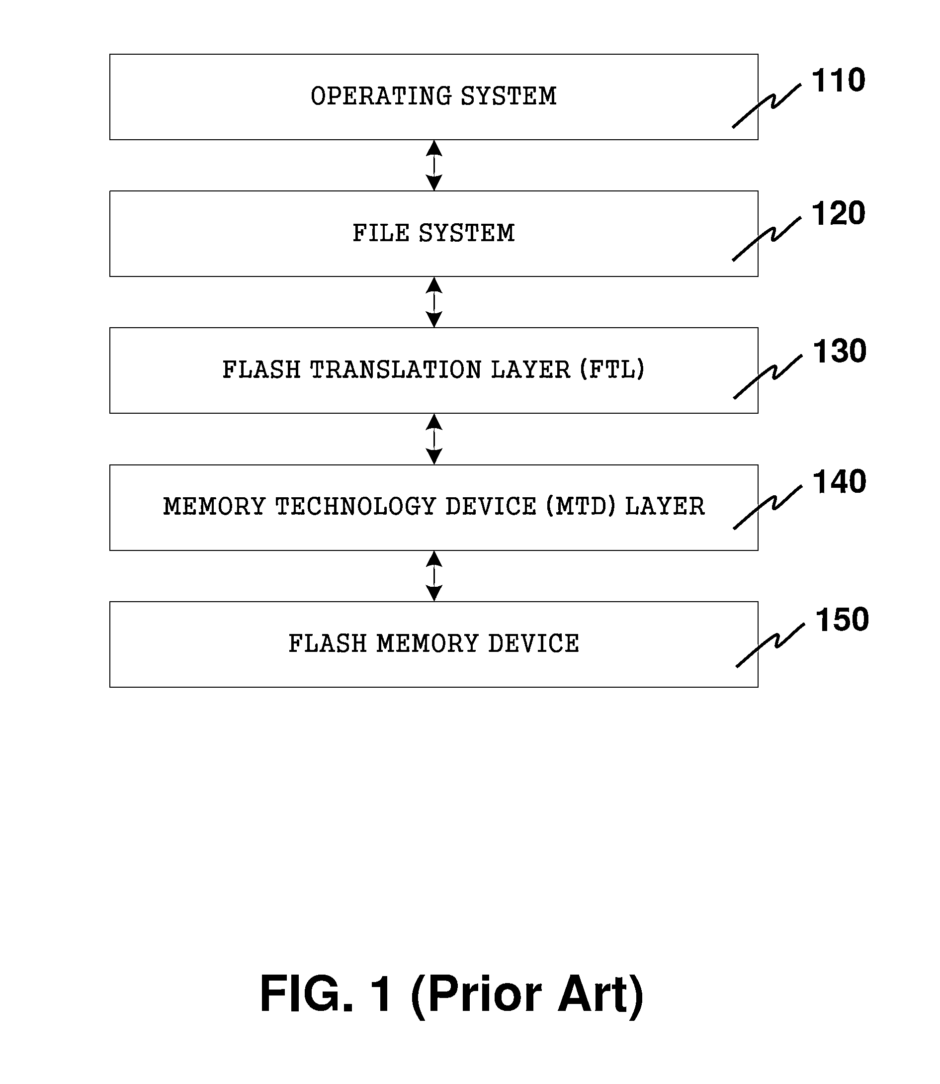
The increasing capacity of NAND flash memory poses tremendous challenges for vendors in the design of block-device emulation software in flash management.
The problem becomes more serious as the capacity of NAND flash memory increases.
Moreover, the page-level mapping table still occupies a lot of space in the

Method used


Image

  • Effective Caching for Demand-based Flash Translation Layers in Large-Scale Flash Memory Storage Systems
  • Effective Caching for Demand-based Flash Translation Layers in Large-Scale Flash Memory Storage Systems
  • Effective Caching for Demand-based Flash Translation Layers in Large-Scale Flash Memory Storage Systems

Examples


Embodiment Construction

A. Basic Idea of the Invention

[0036]In Sections C and D below, two address mapping schemes for large-scale NAND flash storage systems are detailed. These two address mapping schemes serve as embodiments of the present invention. For a system with very limited RAM space (e.g., only one or two kilobytes), we disclose an on-demand address mapping scheme that jointly considers both spatial locality and access frequency. For a system with limited RAM space (e.g., less than several megabytes), a demand-based block-level address mapping scheme with a two-level caching mechanism is disclosed for large-scale NAND flash storage systems.

[0037]The basic idea of the invention is to store the block-level address mapping table in specific pages (called translation pages) in the flash memory, while designing caches in RAM for storing on-demand block-level address mappings. Since the entire block-level address mapping table is stored in the flash memory, and only the address mappings demanded are lo...


PUM


Abstract

This invention discloses methods for implementing a flash translation layer in a computer subsystem comprising a flash memory and a random access memory (RAM). According to one disclosed method, the flash memory comprises data blocks for storing real data and translation blocks for storing address-mapping information. The RAM includes a cache space allocation table and a translation page mapping table. The cache space allocation table may be partitioned into a first cache space and a second cache space. Upon receiving an address-translating request, the cache space allocation table is searched to identify if an address-mapping data structure that matches the request is present. If not, the translation blocks are searched for the matched address-mapping data structure, where the physical page addresses for accessing the translation blocks are provided by the translation page mapping table. The matched address-translating data structure is also used to update the cache space allocation table.

Description

COPYRIGHT NOTICE[0001]A portion of the disclosure of this patent document contains material, which is subject to copyright protection. The copyright owner has no objection to the facsimile reproduction by anyone of the patent document or the patent disclosure, as it appears in the Patent and Trademark Office patent file or records, but otherwise reserves all copyright rights whatsoever.FIELD OF THE INVENTION[0002]The present invention relates generally to an on-demand address mapping scheme for flash memories. In particular, this invention relates to demand-based block-level address mapping schemes with caches for use in large-scale flash storage systems to reduce the RAM footprint.BACKGROUND[0003]A NAND flash memory is widely used as a non-volatile, shock resistant, and low power-consumption storage device. Similar to other storage media, the capacity of flash-memory chips is increasing dramatically and doubled about every two years. The increasing capacity of NAND flash memory pos...

Claims


Application Information

Patent Timeline
IPC IPC(8): G06F12/02
CPCG06F12/0246G06F2212/7201
Inventor SHAO, ZILIQIN, ZHIWEIWANG, YICHEN, RENHAILIU, DUO
Owner THE HONG KONG POLYTECHNIC UNIV
Learn More