
Optical modulator module and semiconductor optical modulator

a technology of optical modulator and module, which is applied in the direction of optics, optical elements, instruments, etc., can solve the problems of increasing the power consumption of the integrated optical modulator, the impedance of the transmission line is related and the power consumption of the modulator changing according to the power consumption of the modulator

Active Publication Date: 2014-08-28
SUMITOMO ELECTRIC IND LTD
View PDF0 Cites 35 Cited by
  • Summary
  • Abstract
  • Description
  • Claims
  • Application Information

AI Technical Summary

Benefits of technology

The semiconductor optical modulator described in this patent has increased the impedance of the waveguide arms, which reduces power consumption. This results in a more efficient optical modulator that can be driven with less electrical signals. Additionally, the optical output ports on the semiconductor modulator are optically coupled to a polarization multiplexing device without wiring lines, which reduces signal loss and improves overall optical performance. The patent also avoids bending transmission lines and differential transmission lines to prevent signal loss and improve device stability and reliability.

Problems solved by technology

The characteristic impedance of the transmission line is related to power consumption of the modulator.
In other words, power consumption of the modulator changes depending on the characteristic impedance of the transmission line.
Therefore, power consumption of the integrated optical modulator increases depending on the number of modulators.
Therefore, it is not easy to avoid an increase in the power consumption of the integrated optical modulator.

Method used


Image

  • Optical modulator module and semiconductor optical modulator
  • Optical modulator module and semiconductor optical modulator
  • Optical modulator module and semiconductor optical modulator

Examples


example

[0100]A stacked semiconductor layer including an n-type contact layer, an n-type lower cladding layer, a core layer (multi-quantum well (MQW) structure), a p-type upper cladding layer, and a p-type contact layer is formed on a semi-insulating InP substrate. For example, the organic-metal vapor phase epitaxy (MOVPE) method is used for epitaxial growth of those semiconductor layers.

One Example of Structure of Stacked Semiconductor Layer

[0101]N-type contact layer: Si-doped n-InP with thickness of 600 nm.

[0102]Lower cladding layer: Si-doped n-InP and i-InP. A dopant concentration of the n-InP is lower than that in the n-type contact layer. A thickness of the n-InP is 780 nm. The n-InP and the i-InP are arranged in the mentioned order in a direction toward the core layer from the substrate. A thickness of the i-InP is 20 nm.

[0103]Core layer: Multi-quantum well (MQW) structure including AlGaInAs layers (well layers) and AlInAs layers (barrier layers) stacked alternately. A thickness of th...


PUM


Abstract

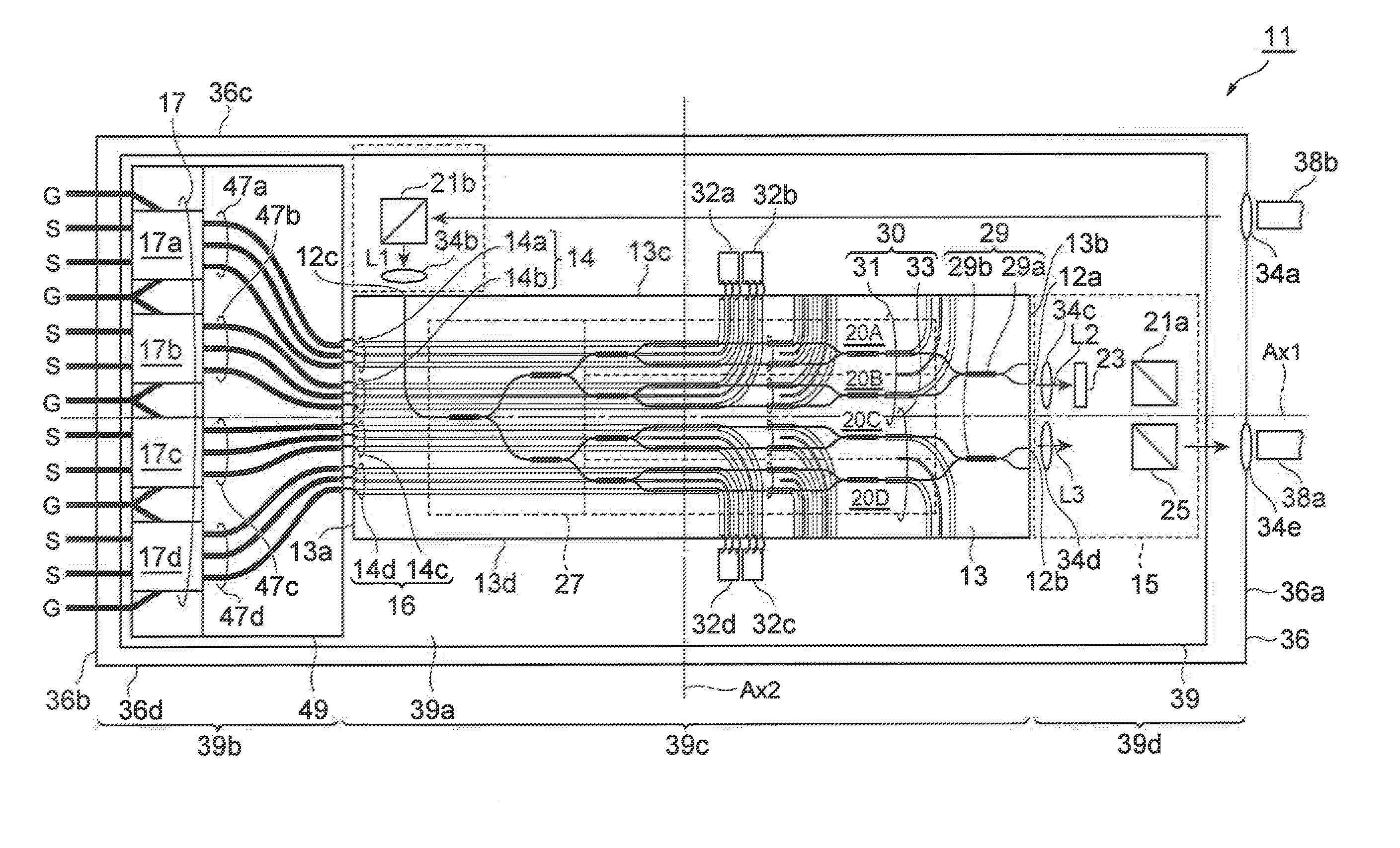
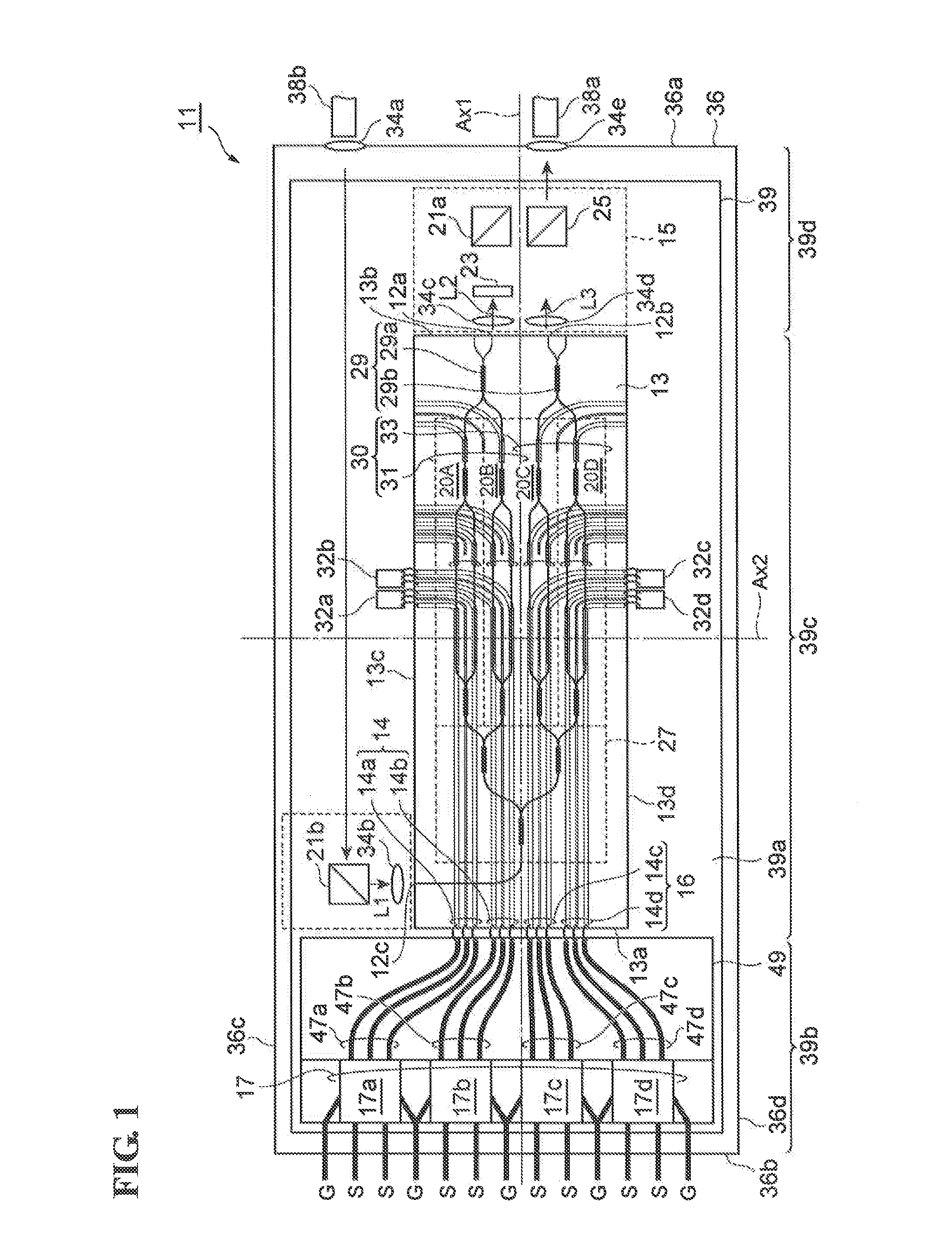
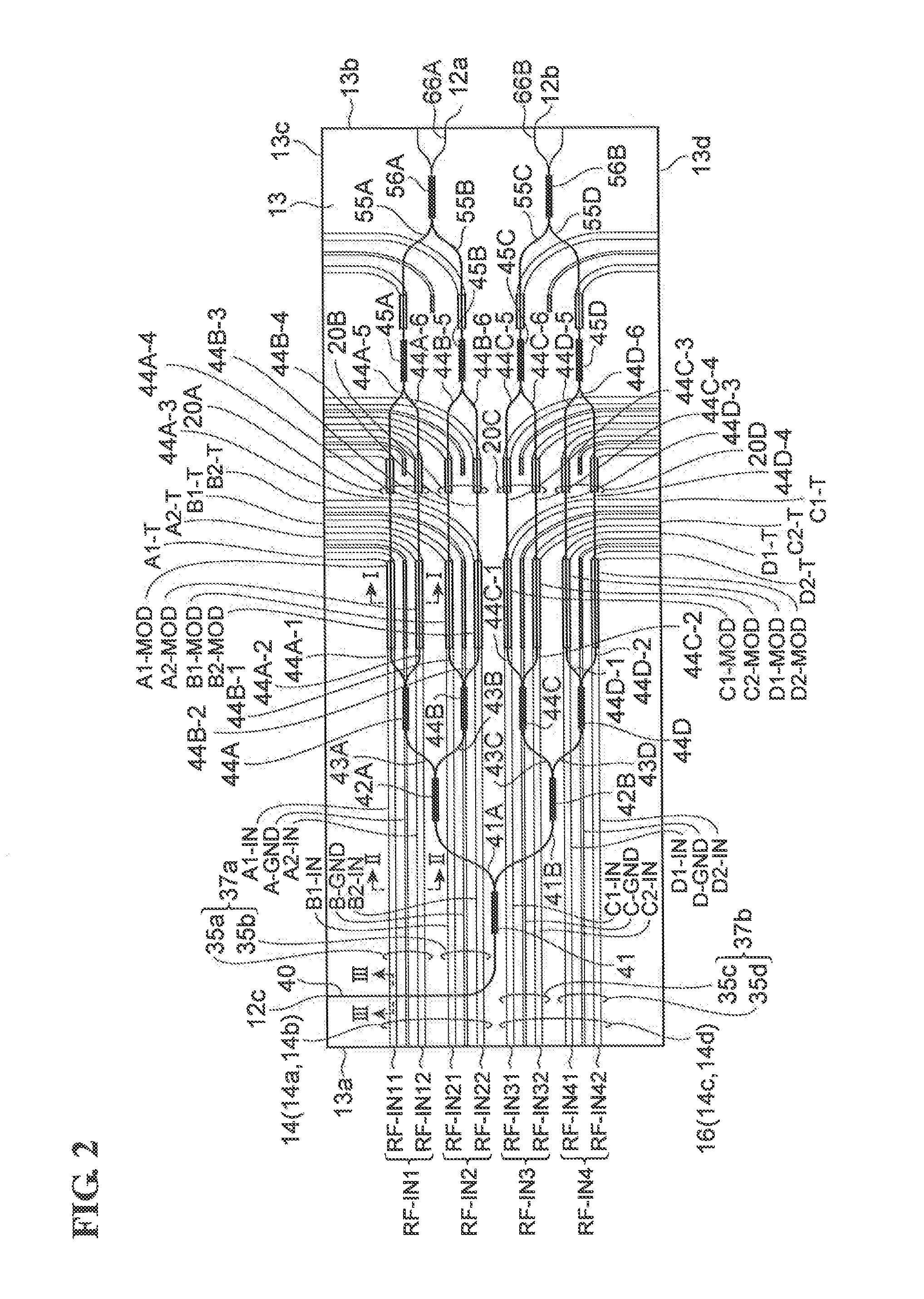
A semiconductor optical modulator includes optical input and output portions; a plurality of Mach-Zehnder modulators including first and second waveguide arms having first and second modulation electrodes, respectively; an optical demultiplexer coupled between the optical input portion and the Mach-Zehnder modulator through an optical waveguide; an optical multiplexer coupled between the optical output portion and the Mach-Zehnder modulator; a plurality of electrical inputs including first, second, and common electrodes disposed between the first and second electrodes; and a plurality of differential transmission lines electrically connecting the electrical inputs to the Mach-Zehnder modulators. The Mach-Zehnder modulators, the optical demultiplexer, the optical multiplexer, the electrical inputs, and the differential transmission lines are disposed on a single substrate. In addition, the first and second modulation electrodes, the electrical inputs, and the differential transmission lines have a differential impedance in a range of 80Ω to 95Ω.

Description

BACKGROUND OF THE INVENTION[0001]1. Field of the Invention[0002]The present invention relates to an optical modulator module and a semiconductor optical modulator.[0003]2. Description of the Related Art[0004]Japanese Patent No. 4235154 and Japanese Unexamined Patent Application Publication No. 2010-008869 disclose InP-based modulators. K.-O. Velthaus, et. al, “High performance InP-based Mach-Zehnder modulators for 10 to 100 Gb / s optical fiber transmission systems,” 23rd International Conference on Indium Phosphide and Related Materials, IPRM 2011, Th-8.1.2 May 22-26, 2011, Berlin, Germany discloses another InP-based modulator.[0005]The above-cited paper discloses an integrated optical device in which four Mach-Zehnder (MZ) modulators are integrated. A modulation signal for the push-pull modulation is applied to the individual waveguide arms through a single-phase transmission line having a characteristic impedance of 50 Ohm (Ω). The modulator is thus modulated by the modulation sign...

Claims


Application Information

Patent Timeline
IPC IPC(8): G02F1/01
CPCG02F1/011G02F1/0121G02B6/29355G02F1/2257H04B10/556
Inventor FUKUDA, CHIEKONO, NAOYASEKI, MORIHIROYAMAJI, KAZUHIROYAMAUCHI, YASUYUKITANAKA, KEIJITATSUMI, TAIZOITABASHI, NAOKI
Owner SUMITOMO ELECTRIC IND LTD
Learn More