
Liquid crystal device and electronic apparatus

a liquid crystal device and electronic equipment technology, applied in the field of liquid crystal devices and electronic equipment, can solve the problems of uneven illumination, difficulty in sufficiently obtaining an effect of improving contrast, and low light use efficiency, and achieve the effect of reducing uneven illumination, high contrast of images projected on screens, and reducing uneven illumination

Inactive Publication Date: 2014-08-07
SEIKO EPSON CORP
View PDF13 Cites 13 Cited by
  • Summary
  • Abstract
  • Description
  • Claims
  • Application Information

AI Technical Summary

Benefits of technology

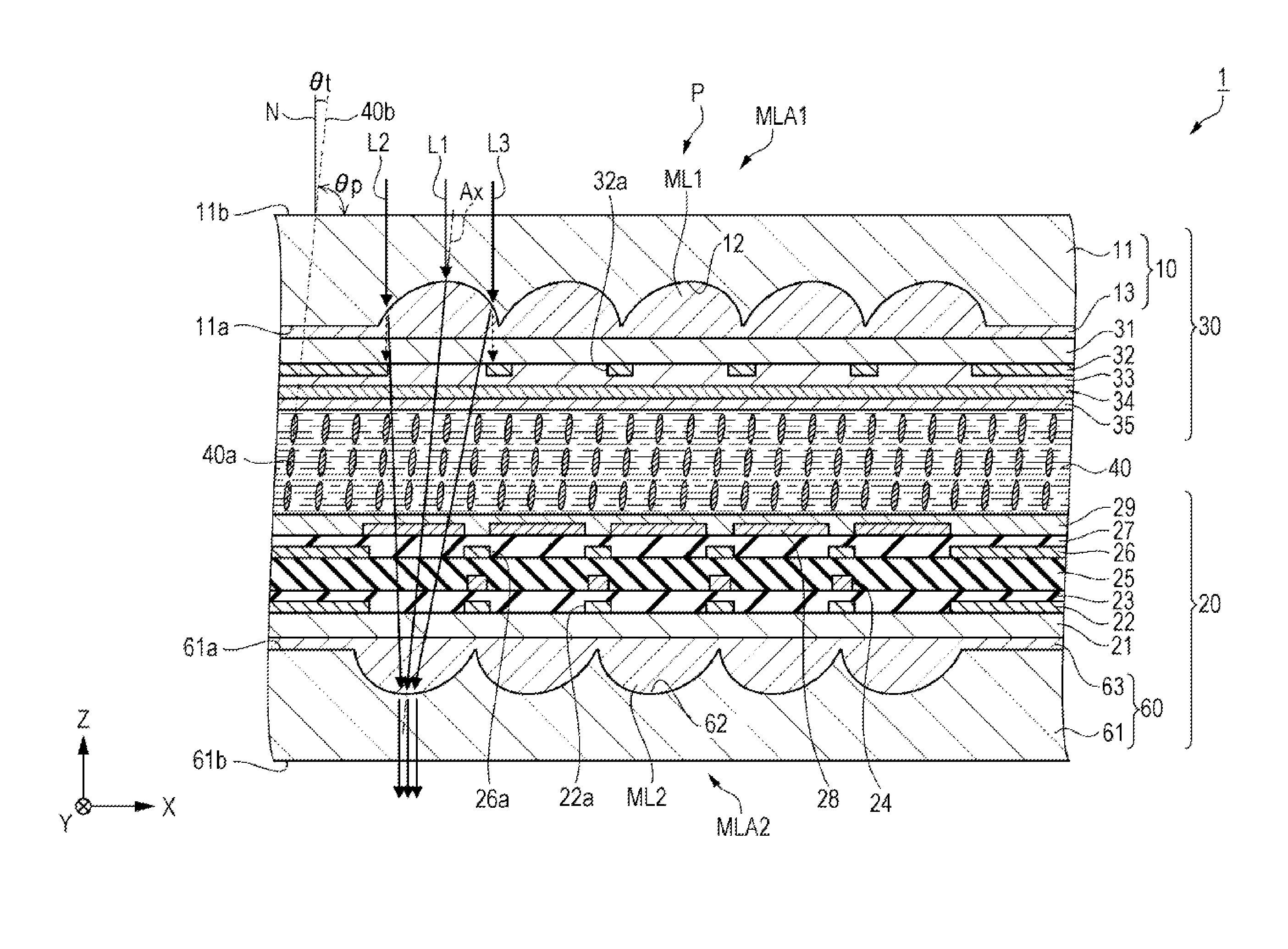
The patent text describes different configurations for an electronic apparatus, such as a liquid crystal device, that can improve its performance. The first configuration involves using a first microlens to condense and tilt the optical axis of input light so that it aligns with the long axis of liquid crystal molecules in the initial aligning state. This allows a large amount of light to penetrate the liquid crystal layer without crossing the optical axis of the first microlens, resulting in improved contrast. The second configuration involves using a second microlens with negative refractive power to refract the light back to the first microlens, reducing uneven illuminance when performing projection on a screen. The third configuration involves separating the edge portions of the first and second openings of a light-blocking layer by a same distance to improve the use efficiency of the light. The electronic apparatus using these configurations can provide high contrast and reduced uneven illuminance.

Problems solved by technology

Accordingly, there is a problem in that transmissivity of the light which penetrates the liquid crystal layer decreases, and it is difficult to sufficiently obtain an effect of improving contrast.
For this reason, there is a problem in that a light amount which passes through an opening portion of the light-blocking layer becomes small, or there is a concern that tilted light may be input to a neighboring pixel region.
Due to this, since the part of light which has penetrated the liquid crystal layer is not used, there is a problem in that a use efficiency of light decreases.

Method used


Image

  • Liquid crystal device and electronic apparatus
  • Liquid crystal device and electronic apparatus
  • Liquid crystal device and electronic apparatus

Examples


first embodiment

Liquid Crystal Device

[0029]Here, an active matrix-type liquid crystal device which includes a thin film transistor (TFT) as a switching element of a pixel will be described as an example. The liquid crystal device is, for example, a device which can be preferably used as an optical modulation element (liquid crystal light bulb) of a projection-type display device (projector), which will be described later.

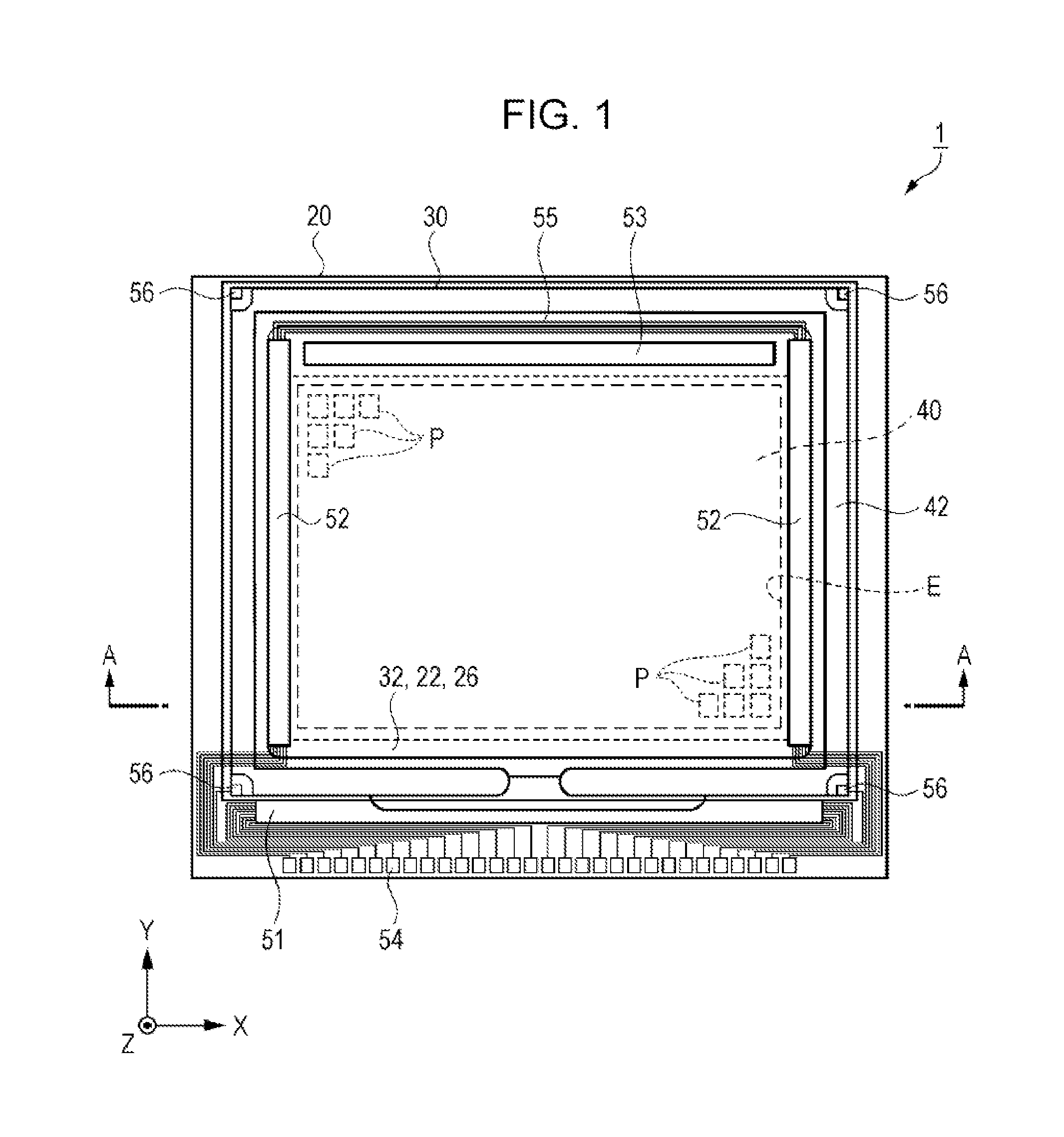
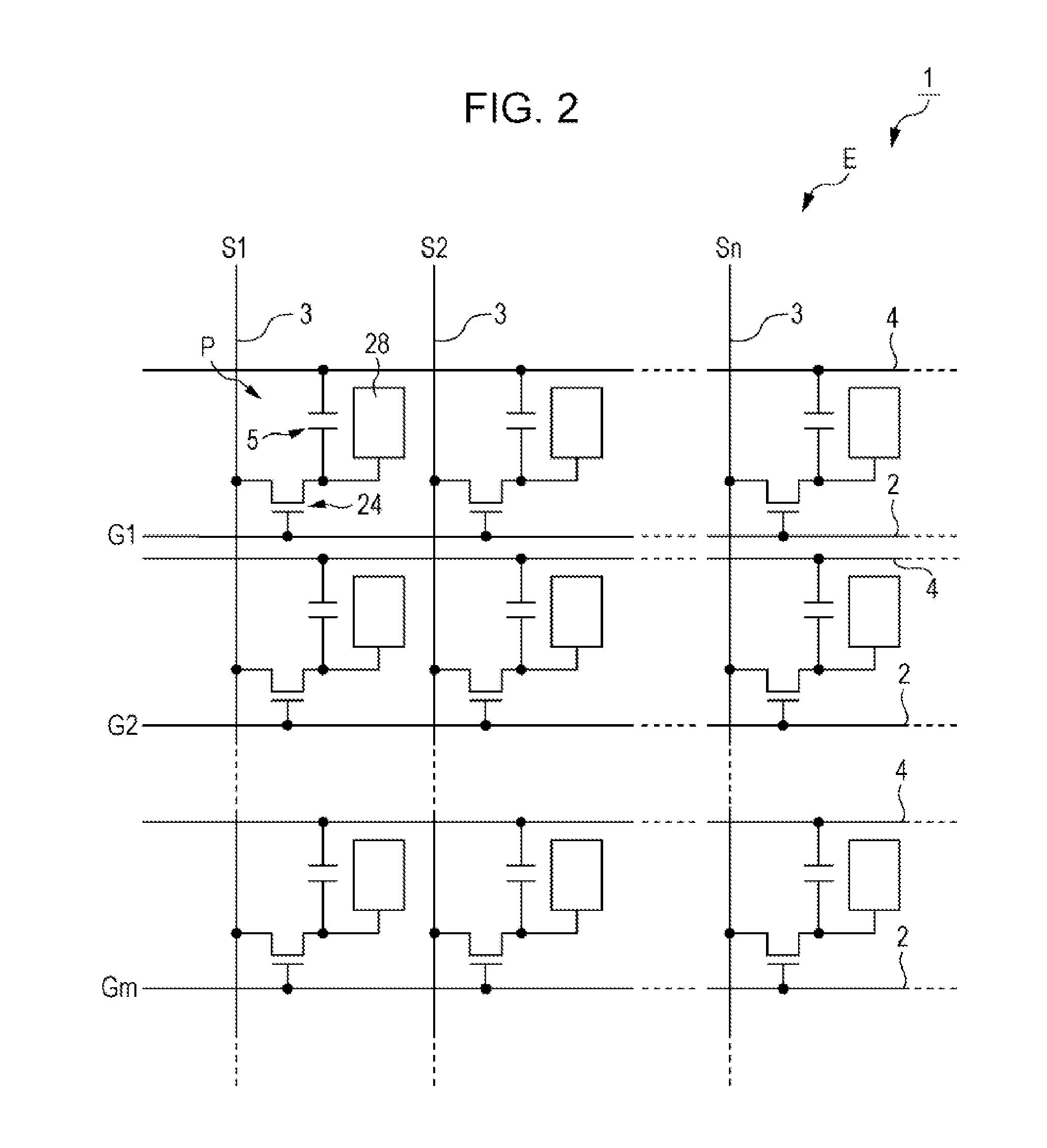
[0030]First, a liquid crystal device according to a first embodiment will be described with reference to FIGS. 1, 2, 3, 4A and 4B, and 5A and 5B. FIG. 1 is a schematic plan view which illustrates a configuration of the liquid crystal device according to the first embodiment. FIG. 2 is an equivalent circuit diagram which illustrates an electrical configuration of the liquid crystal device according to the first embodiment. FIG. 3 is a schematic cross-sectional view which illustrates a configuration of the liquid crystal device according to the first embodiment. More specifically, FI...

second embodiment

Electronic Apparatus

[0109]Subsequently, an electronic apparatus according to a second embodiment will be described with reference to FIG. 8. FIG. 8 is a schematic diagram which illustrates a configuration of a projector as the electronic apparatus according to the second embodiment.

[0110]As illustrated in FIG. 8, a projector (projection type display device) 100 as the electronic apparatus according to the second embodiment includes a polarized light illumination device 110, two dichroic mirrors 104 and 105 as light separation elements, three reflecting mirrors 106, 107, and 108, five relay lenses 111, 112, 113, 114, and 115, three liquid crystal light bulbs 121, 122, and 123, a cross dichroic prism 116 as a photosynthesis element, and a projection lens 117.

[0111]The polarized light illumination device 110 includes, for example, a lamp unit 101 as a light source which is formed of a white light source such as an ultrahigh pressure mercury lamp or a halogen lamp, an integrator lens 10...

modification example

[0119]In the configuration of liquid crystal device 1 according to the above described embodiment, the microlens ML1 of the microlens array substrate 10 and the microlens ML2 of the microlens array substrate 60 have the same shape, and the apex of the lens layer 63 is located on the side which is opposite to the apex of the lens layer 13 with respect to the normal line N of the substrate 11 which passes through the center of the pixel P, however, the invention is not limited to this configuration. The microlenses ML1 and ML2 may have different shapes as long as the lenses have the same function as that in the above described embodiment.

[0120]For example, the lens layer 13 has a curved surface shape which is swollen toward the face 11b side of the substrate 11 to which light is input, and the lens layer 63 has a curved surface shape which is swollen toward the face 61b side of the substrate 61 from which light is output, however, the respective lens layers 13 and 63 may have curved s...


PUM

PropertyMeasurementUnit
pretilt angleaaaaaaaaaa
pretilt angle θpaaaaaaaaaa

Abstract

A liquid crystal device includes a first substrate that is arranged on a light input side; a second substrate that is arranged on a light output side; a liquid crystal layer that is arranged between the first and second substrates; a first microlens that is provided on the first substrate such that an optical axis is tilted to a normal line direction of the first substrate; and a second microlens that is provided on the second substrate such that an optical axis is tilted to a normal line direction of the second substrate, in which a focal point of the first microlens is located on a curved surface of the second microlens, or on the light output side rather than the curved surface.

Description

BACKGROUND[0001]1. Technical Field[0002]The present invention relates to, for example, a liquid crystal device and an electronic apparatus.[0003]2. Related Art[0004]As a liquid crystal device which includes a liquid crystal layer between a pair of substrates, for example, a liquid crystal light bulb of a projector has been known. In such a liquid crystal device, it is desired to realize a high use efficiency of light. Accordingly, for example, a configuration in which light input to a liquid crystal device is condensed, and an improvement of a substantial opening rate of the liquid crystal device is made by including a microlens at least on one side of a pair of substrates has been known.[0005]On the other hand, a liquid crystal device of a vertical alignment (VA) mode has been known as a method which is excellent in light transmittance while securing a wide viewing angle, or a good response speed. The liquid crystal device of the VA mode is configured so that, a liquid crystal of w...

Claims


Application Information

Patent Timeline
Patent Type & Authority Applications(United States)
IPC IPC(8): G02F1/1335
CPCG02F1/133526G02B3/04G02B2003/0093
Inventor NIMURA, TORU
Owner SEIKO EPSON CORP
Learn More