Semiconductor device
a technology of semiconductors and circuits, applied in the field of semiconductor devices, can solve problems such as the difficulty of verification of the operation of logic circuits
- Summary
- Abstract
- Description
- Claims
- Application Information
AI Technical Summary
Benefits of technology
Problems solved by technology
Method used
Image


Examples
embodiment 1
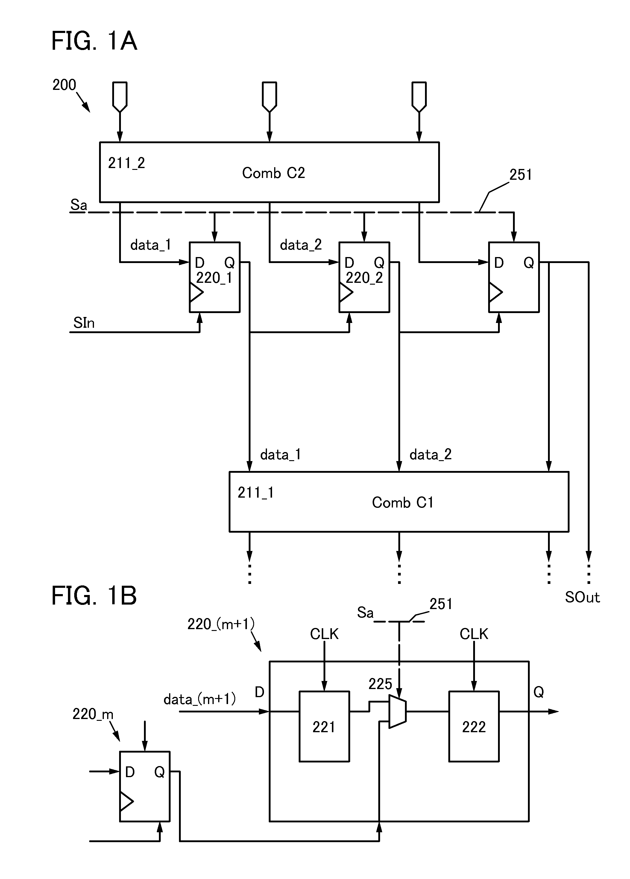
[0044]In this embodiment, the structure of a semiconductor device of one embodiment of the present invention will be described with reference to FIGS. 1A and 1B and FIGS. 2A and 2B.
[0045]FIG. 1A is a block diagram illustrating the structure of a semiconductor device of one embodiment of the present invention. FIG. 1B a block diagram illustrating the structure of the second storage circuit included in the semiconductor device of one embodiment of the present invention.
[0046]A semiconductor device 200 described in this embodiment as an example includes a plurality of storage circuits. Note that for convenience of description, FIG. 1A shows a first storage circuit 220_1 and a second storage circuit 220_2 with their reference number and does not show the other storage circuits.
[0047]FIG. 1A shows a selection signal Sa, a scan-in signal SIn, the scan-out signal SOut, and the clock signal CLK.
[0048]The semiconductor device 200 described in this embodiment as an example includes the first ...
embodiment 2
[0075]In this embodiment, the structure of a semiconductor device of one embodiment of the present invention will be described with reference to FIGS. 3A and 3B and FIG. 4.
[0076]FIG. 3A is a block diagram illustrating the structure of a semiconductor device of one embodiment of the present invention. FIG. 3B is a block diagram illustrating the structure of the second storage circuit included in the semiconductor device of one embodiment of the present invention.
[0077]A semiconductor device 300 described in this embodiment as an example includes a plurality of storage circuits. Note that for convenience of description, FIG. 3A shows a first storage circuit 320_1 and a second storage circuit 320_2 with their reference number and does not show the other storage circuits.
[0078]FIG. 3A shows a first selection signal Sa, a second selection signal Sb, the scan-in signal SIn, the scan-out signal SOut, and the clock signal CLK. FIG. 3A also shows a first control signal BK and a second contro...
embodiment 3
[0117]A storage circuit which retains written data even after the supply of a power supply voltage is stopped can be used as a secondary storage circuit of the semiconductor device 300 of one embodiment of the present invention.
[0118]The semiconductor device 300 of one embodiment of the present invention in which a secondary storage circuit which retains written data even after the supply of a power supply voltage is stopped is used can restart the operation based on data stored before the supply of the power supply voltage is stopped, by supplying the power supply voltage again even when the supply of a power supply voltage is stopped after the supply of the power supply voltage. Therefore, a semiconductor device in which power consumed in retaining data when the supply of the power supply voltage is stopped is low can be provided.
[0119]In this embodiment, a driving method of the secondary storage circuit 330_(m+1) which can be used in the semiconductor device 300 of one embodiment...
PUM
 Abstract
Description
Claims
Application Information
 - R&D
- Intellectual Property
- Life Sciences
- Materials
- Tech Scout
- Unparalleled Data Quality
- Higher Quality Content
- 60% Fewer Hallucinations
Browse by: Latest US Patents, China's latest patents, Technical Efficacy Thesaurus, Application Domain, Technology Topic, Popular Technical Reports.
© 2025 PatSnap. All rights reserved.Legal|Privacy policy|Modern Slavery Act Transparency Statement|Sitemap|About US| Contact US: help@patsnap.com