Contact pad structure
- Summary
- Abstract
- Description
- Claims
- Application Information
AI Technical Summary
Benefits of technology
Problems solved by technology
Method used
Image
Examples
first embodiment
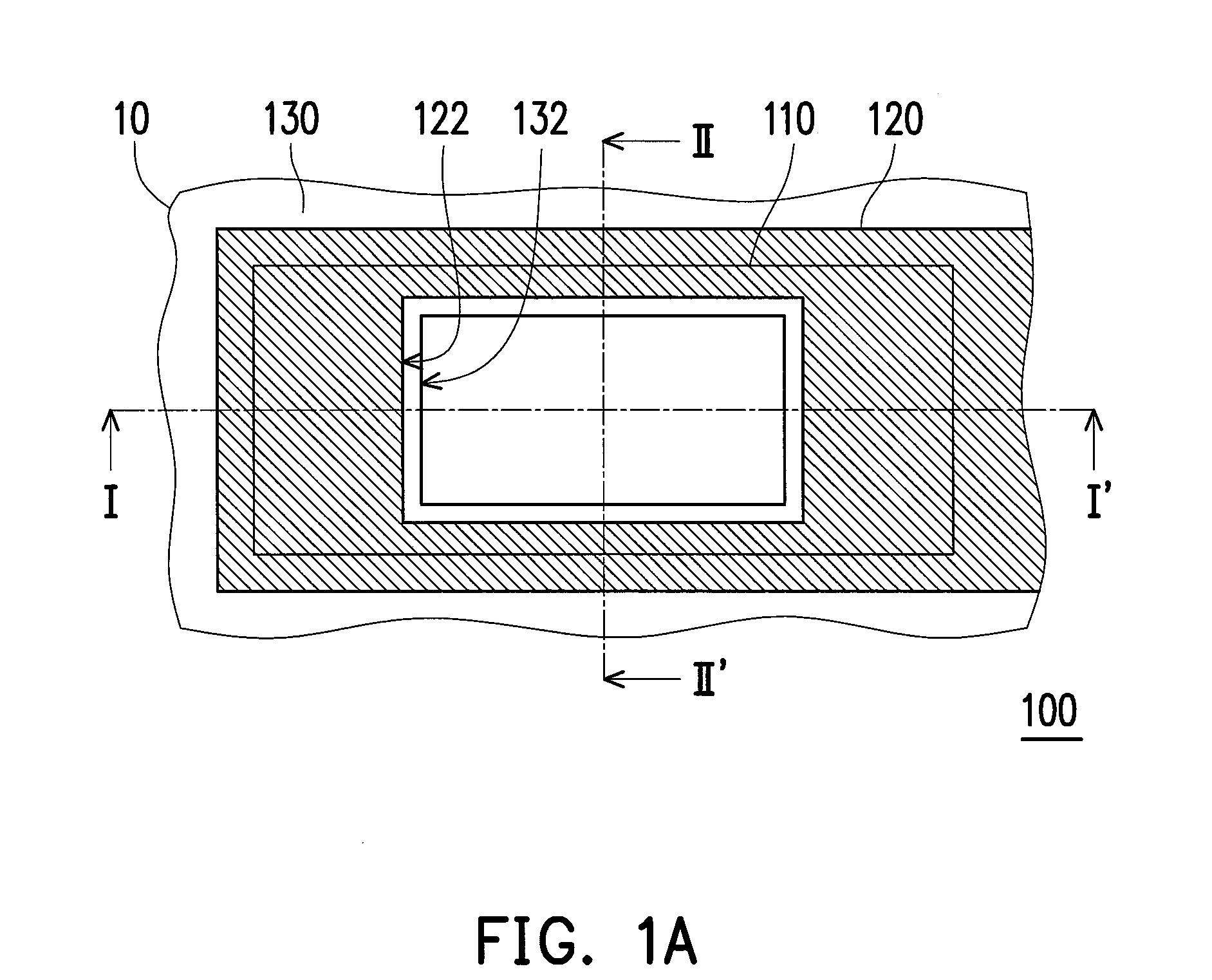
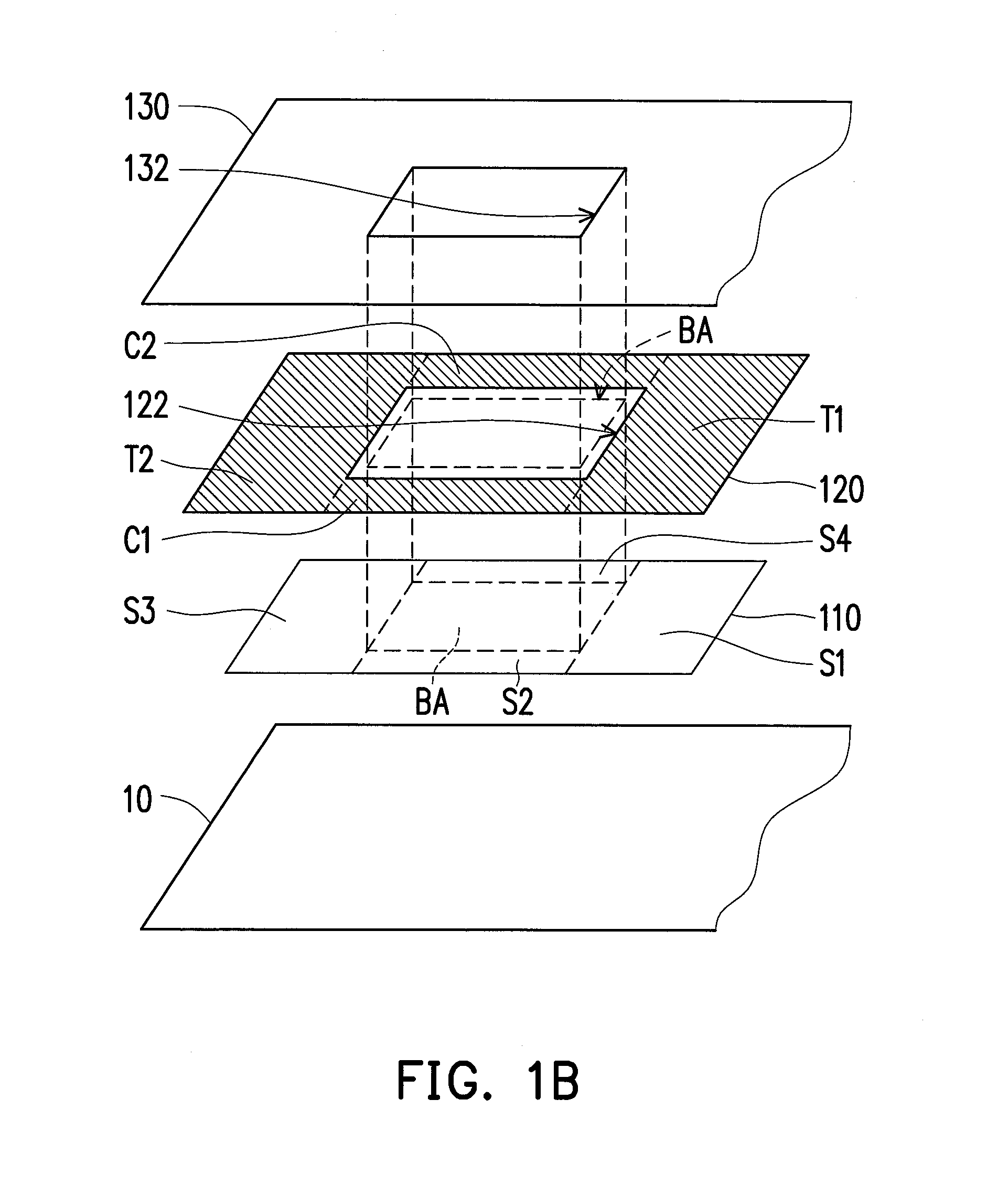
[0031]FIG. 1A is a schematic top view showing a contact pad structure according to the present invention and FIG. 1B is a schematic exploded view showing each part of the contact pad structure depicted in FIG. 1A. Referring to both FIGS. 1A and 1B, the contact pad structure 100 is disposed on a substrate 10 and the contact pad structure 100 includes a transparent conductive pattern 110, a metal conductive pattern 120 and a protection layer 130 which are sequentially stacked on the substrate 10. In the embodiment, the protection layer 130 can be made of insulation material such as organic material, inorganic material (SiO2 or SiNx) and so on. Accordingly, the transparent conductive layer 110 is located between the metal conductive pattern 120 and the substrate 10 and the transparent conductive pattern 110 and the metal conductive pattern 120 are both located between the protection layer 130 and the substrate 10.
[0032]The transparent conductive pattern 110 of the present embodiment ha...
second embodiment
[0038]It should be noted that although the embodiment uses the first connection region C1 and the second connection region C2 of the metal conductive pattern 120 in contact with the transparent conductive pattern 110 as an example, the present invention is not limited thereto. FIG. 2A is a schematic top view showing a contact pad structure according to the present invention and FIG. 2B is a schematic cross-sectional view showing the contact pad structure taken along the line III-III′ of FIG. 2A. Referring to both FIGS. 2A and 2B, the contact pad structure 200 is disposed on a substrate 10 and the contact pad structure 200 includes a transparent conductive pattern 110, a metal conductive pattern 220 and a protection layer 130, in which the structural designs of the substrate 10, the transparent conductive pattern 110 and the protection layer 130 can be referred to the above embodiment and are not reiterated hereinafter. In the present embodiment, the metal conductive pattern 220 has ...
third embodiment
[0040]It should be noted that although the embodiment depicted in FIG. 1A through FIG. 1D uses the metal conductive pattern 120 completely surrounding the bonding region BA and having the closed metal pattern opening 122 as an example, the present invention is not limited thereto. FIG. 3A is a schematic top view showing a contact pad structure according to the present invention and FIG. 3B is a schematic cross-sectional view showing the contact pad structure taken along the line IV-IV′ of FIG. 3A. Referring to both FIGS. 3A and 3B, the contact pad structure 300 is disposed on a substrate 10 and the contact pad structure 300 includes a transparent conductive pattern 110, a metal conductive pattern 320 and a protection layer 130, in which the structural designs of the substrate 10, the transparent conductive pattern 110 and the protection layer 130 can be referred to the above embodiment and are not reiterated hereinafter. In the present embodiment, the metal conductive pattern 320 ha...
PUM
 Abstract
Description
Claims
Application Information
 - R&D
- Intellectual Property
- Life Sciences
- Materials
- Tech Scout
- Unparalleled Data Quality
- Higher Quality Content
- 60% Fewer Hallucinations
Browse by: Latest US Patents, China's latest patents, Technical Efficacy Thesaurus, Application Domain, Technology Topic, Popular Technical Reports.
© 2025 PatSnap. All rights reserved.Legal|Privacy policy|Modern Slavery Act Transparency Statement|Sitemap|About US| Contact US: help@patsnap.com


