
Semiconductor materials, transistors including the same, and electronic devices including transistors

a technology of semiconductor materials and transistors, applied in the direction of discharge tube main electrodes, conductors, instruments, etc., can solve the problems of limiting the operating speed of a display apparatus including an amorphous silicon tft, reducing image quality, and high manufacturing process and cost of amorphous silicon tft, etc., to achieve excellent switching characteristics and high mobility

Active Publication Date: 2014-06-05
SAMSUNG ELECTRONICS CO LTD +1
View PDF7 Cites 21 Cited by
  • Summary
  • Abstract
  • Description
  • Claims
  • Application Information

AI Technical Summary

Benefits of technology

This patent is about making transistors that have very good mobility and can switch quickly. This is important for making electronic devices that can perform their tasks efficiently.

Problems solved by technology

An amorphous silicon TFT may have a charge mobility of about 0.5 cm2 / Vs or so, which is so low and may limit an operating speed of a display apparatus including an amorphous silicon TFT.
As a result, manufacturing processes and costs for a polycrystalline silicone TFT may be higher than those for an amorphous silicon TFT.
Also, it may be difficult to ensure uniformity of a polycrystalline silicon layer in the polycrystalline silicon TFT; consequently, image quality may be reduced when the polycrystalline silicon layer is used as a channel layer of a large-size display apparatus.
However, a conventional oxide TFT may not ensure excellent switching characteristics (e.g., ON / OFF characteristics) and high reliability.

Method used


Image

  • Semiconductor materials, transistors including the same, and electronic devices including transistors
  • Semiconductor materials, transistors including the same, and electronic devices including transistors
  • Semiconductor materials, transistors including the same, and electronic devices including transistors

Examples


Embodiment Construction

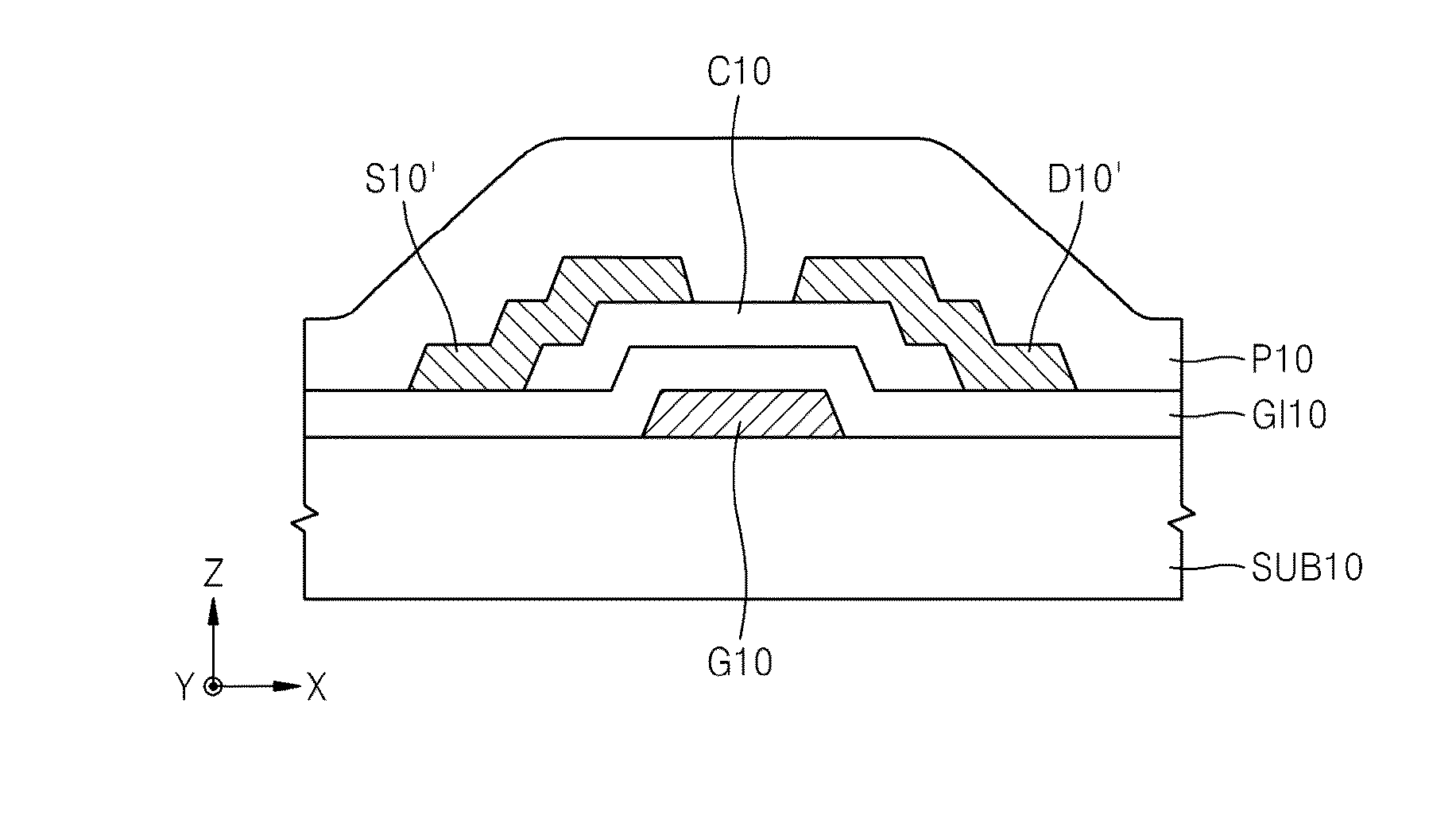
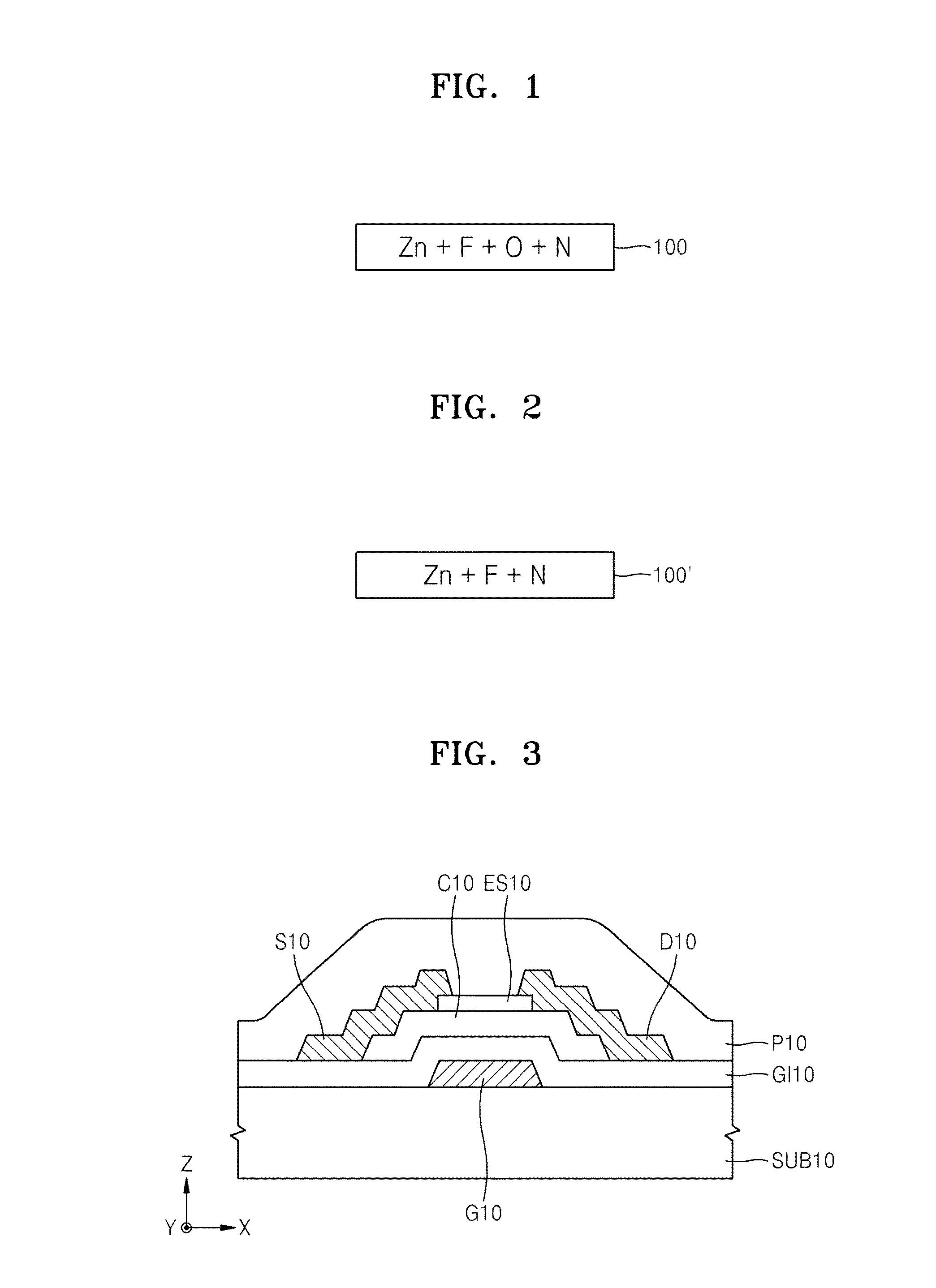
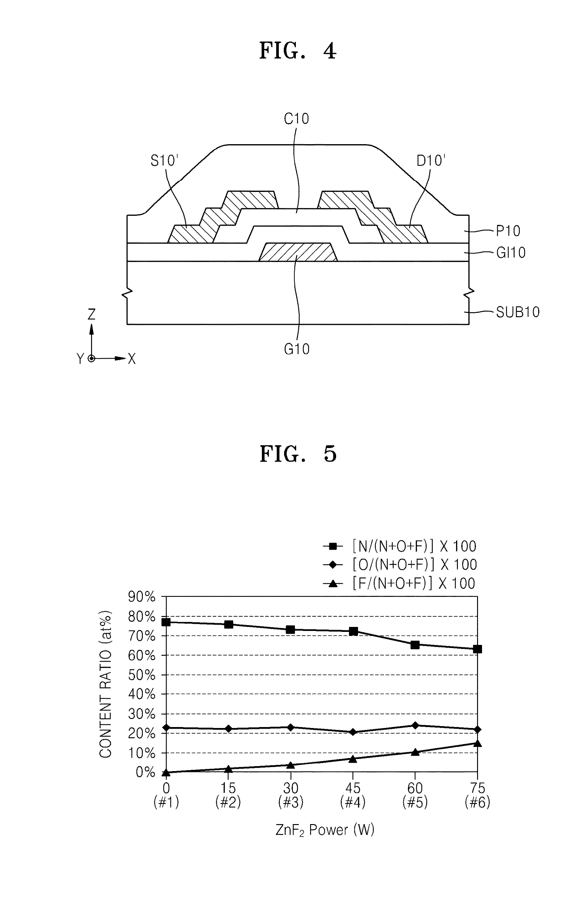
[0164]Example embodiments will now be described more fully with reference to the accompanying drawings, in which some example embodiments are shown. Example embodiments, may, however, be embodied in many different forms and should not be construed as being limited to the embodiments set forth herein; rather, these example embodiments are provided so that this disclosure will be thorough and complete, and will fully convey the scope of example embodiments of inventive concepts to those of ordinary skill in the art. In the drawings, the thicknesses of layers and regions are exaggerated for clarity. Like reference numerals in the drawings denote like elements, and thus their description may be omitted.

[0165]It will be understood that when an element is referred to as being “connected” or “coupled” to another element, it can be directly connected or coupled to the other element or intervening elements may be present. In contrast, when an element is referred to as being “directly connect...


PUM

PropertyMeasurementUnit
pressureaaaaaaaaaa
temperatureaaaaaaaaaa

Abstract

According to example embodiments, a semiconductor material may include zinc, nitrogen, and fluorine. The semiconductor material may further include oxygen. The semiconductor material may include a compound. For example, the semiconductor material may include zinc fluorooxynitride. The semiconductor material may include zinc oxynitride containing fluorine. The semiconductor material may include zinc fluoronitride. The semiconductor material may be applied as a channel material of a thin film transistor (TFT).

Description

CROSS-REFERENCE TO RELATED APPLICATIONS[0001]This application is a continuation of U.S. application Ser. No. 14 / 093,121, filed on Nov. 29, 2013, which claims priority under 35 U.S.C. §119 to Korean Patent Application Nos. 10-2012-0138508 and 10-2013-0097345, respectively filed on Nov. 30, 2012 and Aug. 16, 2013, in the Korean Intellectual Property Office, the disclosures of which are incorporated herein in their entirety by reference.BACKGROUND[0002]1. Field[0003]Example embodiments relate to semiconductor materials and / or devices including the same, and more particularly, to semiconductor materials, transistors including the same, and / or electronic devices including the transistors.[0004]2. Description of Related Art[0005]Transistors are widely used as switching devices and / or driving devices in electronic devices. In particular, since a thin film transistor (TFT) may be manufactured on a glass substrate or a plastic substrate, TFTs may be used in display apparatuses such as organi...

Claims


Application Information

Patent Timeline
Patent Type & Authority Applications(United States)
IPC IPC(8): H01L29/786H05B44/00
CPCH01L29/7869H01L29/78693H01L29/78696H01L29/24
Inventor KIM, TAE-SANGKIM, SUN-JAEKIM, HYUN-SUKRYU, MYUNG-KWANPARK, JOON-SEOKSEO, SEOK-JUNSEON, JONG-BAEKSON, KYOUNG-SEOK
Owner SAMSUNG ELECTRONICS CO LTD
Learn More