Power Semiconductor Housing With Contact Mechanism

a technology of contact mechanism and semiconductor housing, which is applied in the direction of emergency protective devices, electronic switching, pulse techniques, etc., can solve the problems of power transmission and unnecessary disruption, and achieve the effect of avoiding accidental activation

Inactive Publication Date: 2014-05-29
ABB POWER GRIDS SWITZERLAND AG
View PDF5 Cites 3 Cited by
  • Summary
  • Abstract
  • Description
  • Claims
  • Application Information

AI Technical Summary

Benefits of technology

The invention provides a housing for installing a power semiconductor with a bypass that can quickly and reliably activate in case of an explosion. The bypass is designed to prevent accidental activation and can remain active for as long as necessary.

Problems solved by technology

A problem with such bypassing devices, which includes bypassing means that are released during a failure, is that they may also be released accidentily without any failure and cause unnecessary disruption of. for example, power transmission.

Method used


Image

  • Power Semiconductor Housing With Contact Mechanism
  • Power Semiconductor Housing With Contact Mechanism
  • Power Semiconductor Housing With Contact Mechanism

Examples


Embodiment Construction

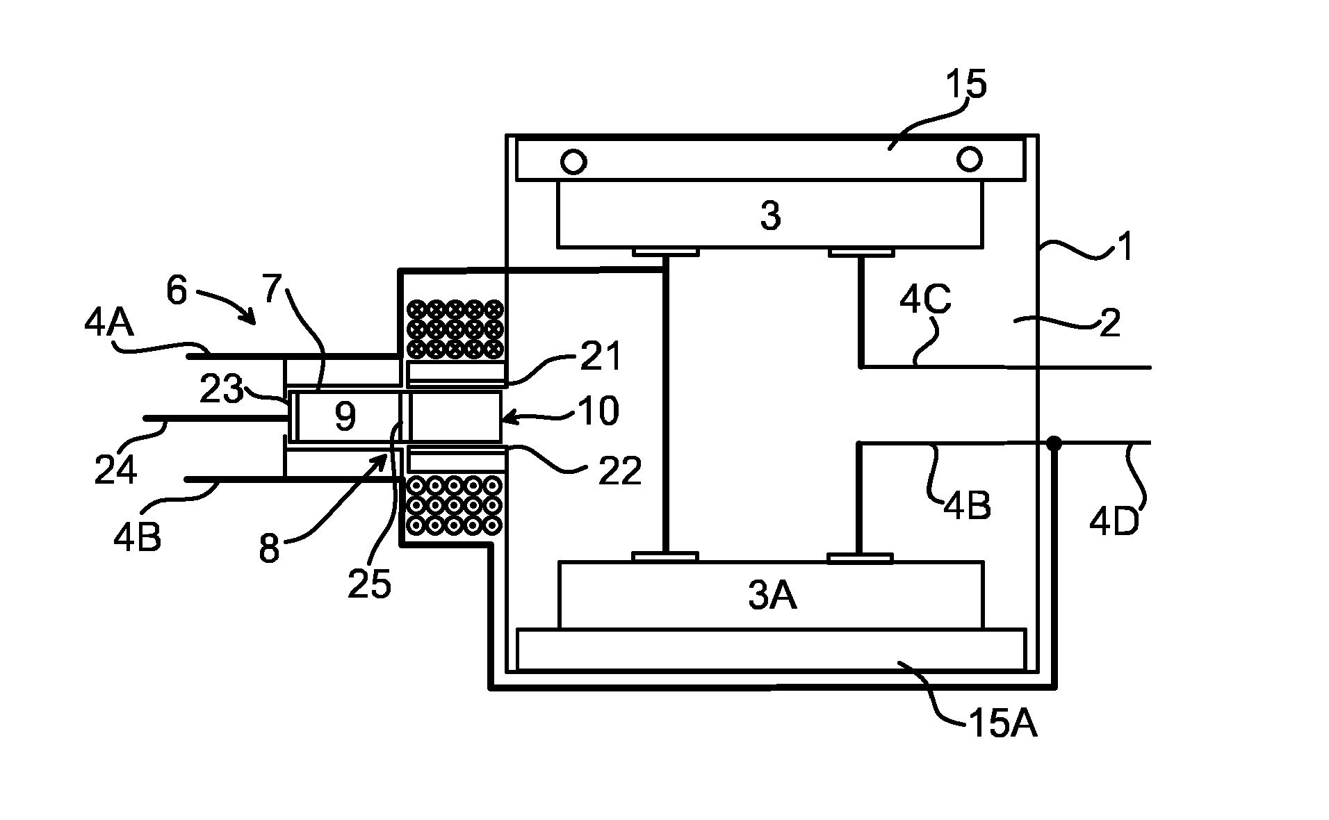
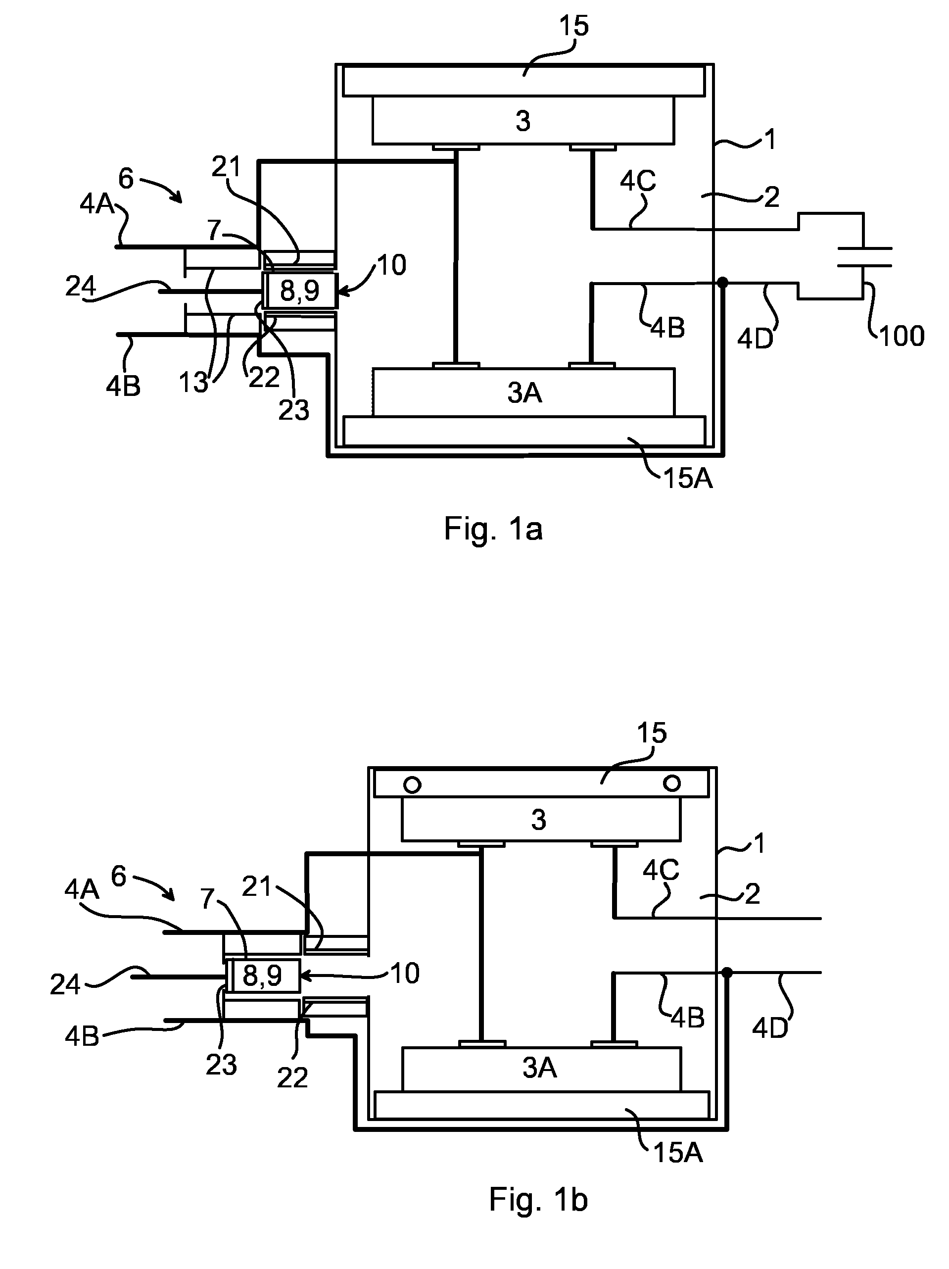
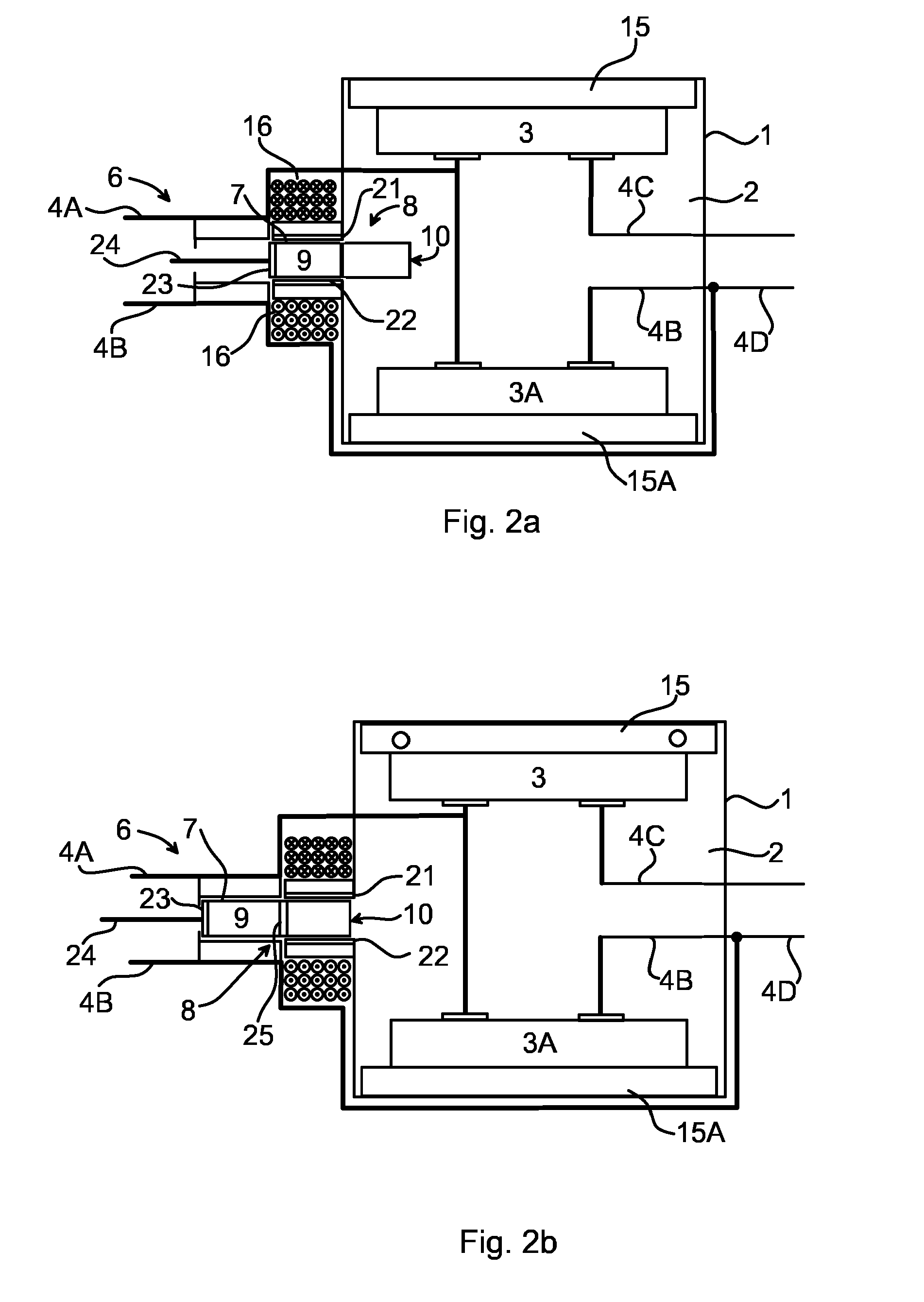
[0033]FIG. 1a and FIG. 1b illustrates a first embodiment of the housing 1 according to the present invention. The housing 1 surrounds a compartment 2 with mounting plates 15, 15A for installation of a respective power semiconductor 3, 3A. The power semiconductor device 3, 3A is referred to as a “power semiconductor” but may include other components, such as is known in the art and which device includes least one power semiconductor switch, such as an IGBT, or GTO. The installations of FIGS. 1A and 1B include two power semiconductors 3, 3A. The housing 1 is provided with terminals 4A, 4B, 4C for leading electrical currents to and from each of the power semiconductors 3, 3A. The housing includes two terminals 4A, 4B arranged for leading current into and out of the housing 1, each terminal 4A, 4B having one end outside the housing, for connecting to a busbar conductor of, for example, a converter system. Each terminal 4A, 4B extends into the housing 1 and has a second end inside the ho...


PUM


Abstract

A housing for a power semiconductor, providing a compartment for installation of a power semiconductor, and including a first and a second terminal. The terminals are for connection of a power semiconductor installed in the compartment, and for leading current to and from the compartment. The housing includes a contact mechanism for bypassing the compartment, the contact mechanism including at least one movable contact arranged for electrically connecting the first and second terminal, the at least one movable contact being movable between a disconnected first position and a connected second position. The contact mechanism further includes a bypass actuator arranged inside the compartment and provided for transforming a pressure from an exploding semiconductor into motion, the bypass actuator is operatively connected to the movable contact and arranged to move the movable contact from the first to the second position when subjected to the pressure of an exploding semiconductor.

Description

FIELD OF THE INVENTION[0001]The invention relates to electrical power systems comprising power semiconductors and especially for protection against damage and malfunctioning caused by exploding power semiconductors.BACKGROUND OF THE INVENTION[0002]The invention relates protection against damage and malfunctioning caused by exploding power semiconductors. Especially, the invention relates to installations for bypassing an exploded power semiconductor, such as an IGBT.[0003]Power semiconductors, such as IGBTs (Insulated Gate Bipolar Transistor) or GTOs (Gate Turnoff Thyristor), are used in the field of power transmission systems for converting electrical current. In such systems, a series of modules comprising a semiconductor may be arranged in branch, one for each phase, of a converter. Such converters are used for conversion between AC and DC. In the event of a malfunctioning semiconductor, such systems have been adapted to bridge or bypass this faulty semiconductor or the installat...

Claims


Application Information

Patent Timeline
IPC IPC(8): H01L23/00
CPCH01H79/00H01L23/04H01L25/074H01L25/115H01L2924/13055H01L2924/16151H01L2924/17151H02M7/003H01H39/004H03K17/107H01L2924/0002H01L2924/00H01L23/562
Inventor MONGE, MAURO
Owner ABB POWER GRIDS SWITZERLAND AG
Why Eureka
Try Eureka