Semiconductor device
- Summary
- Abstract
- Description
- Claims
- Application Information
AI Technical Summary
Benefits of technology
Problems solved by technology
Method used
Image
Examples
embodiment 1
[0067]In this embodiment, a transistor 100 is described as an example of a semiconductor device.
[1-1. Structural Example of Semiconductor Device]
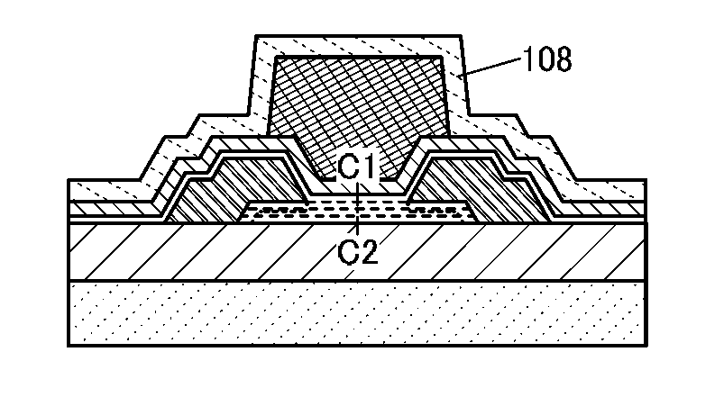
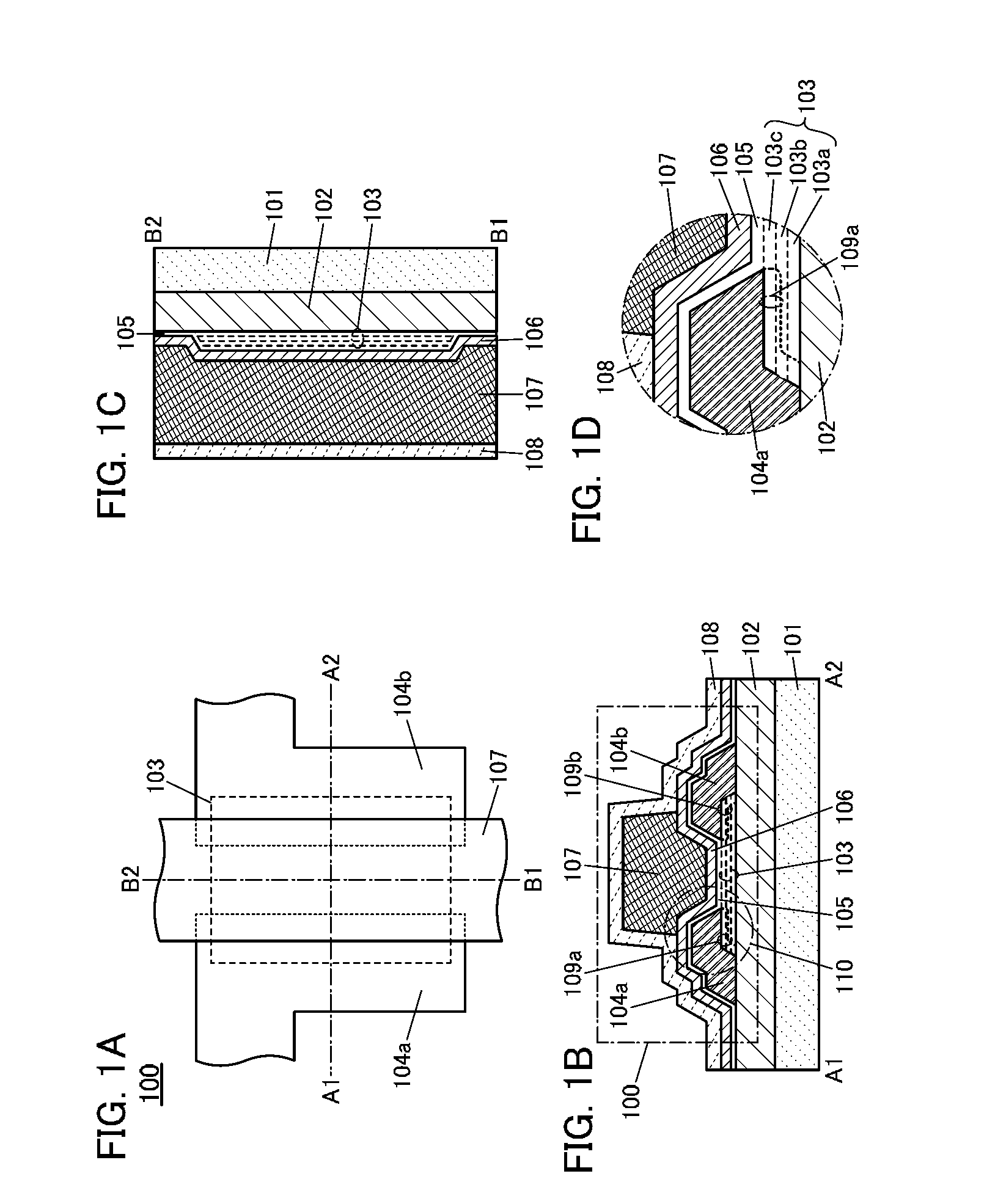
[0068]FIGS. 1A to 1D illustrate the transistor 100 of one embodiment of a semiconductor device. The transistor 100 is a top-gate transistor. FIG. 1A is a top view of the transistor 100. FIG. 1B is a cross-sectional view of a portion denoted by a dashed dotted line A1-A2 in FIG. 1A and FIG. 1C is a cross-sectional view of a portion denoted by a dashed dotted line B1-B2 in FIG. 1A. FIG. 1D is an enlarged view of a portion 110 in FIG. 1B. Note that some components are not illustrated in FIG. 1A.
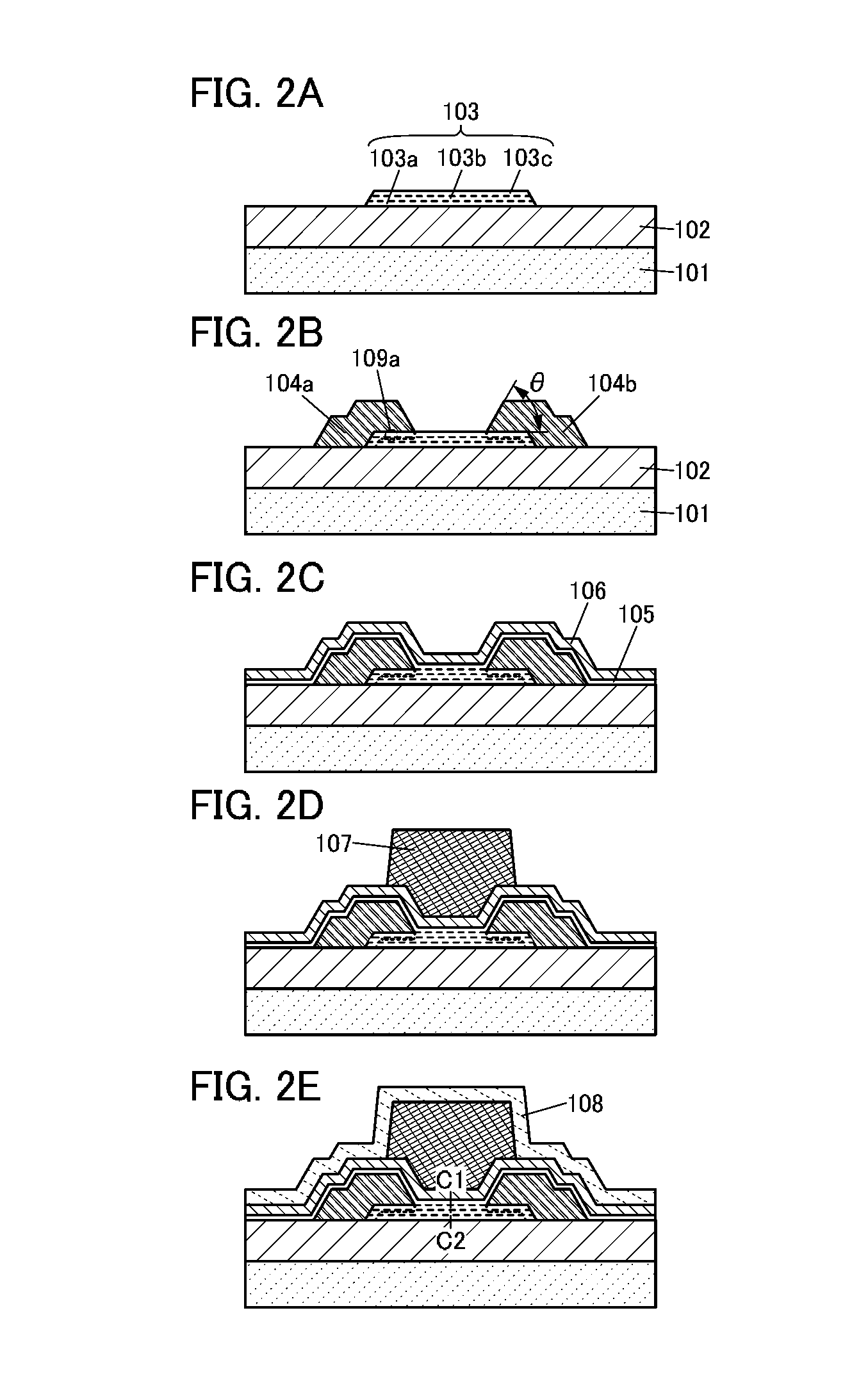
[0069]The transistor 100 is formed over an insulating layer 102. The insulating layer 102 is formed over a substrate 101. The transistor 100 includes a stack 103 which is formed over the insulating layer 102 and includes a source electrode 104a and a drain electrode 104b which are formed over the stack 103. An oxide layer 105 is formed over the source e...
embodiment 2
[0273]In this embodiment, a transistor 150 which has a different structure from the transistor 100 described in the above embodiment is described.
[2-1. Structural Example of Semiconductor Device]
[0274]FIGS. 11A to 11C illustrate the transistor 150 of one embodiment of a semiconductor device. FIG. 11A is a top view of the transistor 150. FIG. 11B is a cross-sectional view of a portion denoted by a dashed dotted line A3-A4 in FIG. 11A and FIG. 11C is a cross-sectional view of a portion denoted by a dashed dotted line B3-B4 in FIG. 11A.
[0275]The transistor 150 is a top-gate transistor. The transistor 150 has substantially the same structure as the transistor 100 except the shapes of the insulating layer 106 and the oxide layer 105 in a cross-sectional structure.
[0276]The transistor 150 has a structure in which part of the insulating layer 106 and part of the oxide layer 105 which do not overlap with the gate electrode 107 are removed. Such a structure can prevent an increase in leakage...
embodiment 3
[0280]In this embodiment, a transistor 160 which has a different structure from the transistor described in the above embodiment is described.
[3-1. Structural Example of Semiconductor Device]
[0281]FIGS. 12A to 12C illustrate the transistor 160 of one embodiment of the present invention. FIG. 12A is a top view of the transistor 160. FIG. 12B is a cross-sectional view of a portion denoted by a dashed dotted line A5-A6 in FIG. 12A, and FIG. 12C is a cross-sectional view of a portion denoted by a dashed dotted line B5-B6 in FIG. 12A.
[0282]The transistor 160 is a top-gate transistor. The transistor 160 has substantially the same structure as the transistor 100 except the cross-sectional shapes of a source electrode and a drain electrode.
[0283]The edges of a source electrode 104as and a drain electrode 104bs in the transistor 160 each have a step-like shape. The step-like edges of the source electrode 104as and the drain electrode 104bs can lead to an improvement in coverage with a layer ...
PUM
 Abstract
Description
Claims
Application Information
 - R&D
- Intellectual Property
- Life Sciences
- Materials
- Tech Scout
- Unparalleled Data Quality
- Higher Quality Content
- 60% Fewer Hallucinations
Browse by: Latest US Patents, China's latest patents, Technical Efficacy Thesaurus, Application Domain, Technology Topic, Popular Technical Reports.
© 2025 PatSnap. All rights reserved.Legal|Privacy policy|Modern Slavery Act Transparency Statement|Sitemap|About US| Contact US: help@patsnap.com


