Optical element and production of same

a technology of optical elements and production methods, applied in the field of optical elements and production of same, can solve the problems of high production cost, limit the degree of miniaturization that may be performed, and low cost, and achieve the effect of low cost and simple production method

Inactive Publication Date: 2014-05-08
ALBERT LUDWIGS UNIV FREIBURG +1
View PDF7 Cites 5 Cited by
  • Summary
  • Abstract
  • Description
  • Claims
  • Application Information

AI Technical Summary

Benefits of technology

The present invention is based on the finding that the surface function of an optical element can be created by structuring a carrier layer and filling it with a material that cures during production. The surface structure of the optical surface is influenced by the curing-induced shrinkage of the layer comprising the curing material. The invention provides a simple design, which has advantageous effects both with regard to production and with regard to the possibility of miniaturization while exhibiting a large amount of flexibility with regard to the surface function. The optical element can also include a mirror layer arranged on the surface of the layer, which can be shaped in accordance with any surface functions. The layer thickness profile of the layer can be varied, during operation, so that the surface functions influencing the optical properties are directly adaptable during operation. The production method is simple and low in cost.

Problems solved by technology

Such optical elements based on a membrane with an air gap located behind it often involve a large amount of effort in terms of production, which results in high production cost.
In addition, there are limits to the degree of miniaturization that may be performed.
Consequently, this production method is simple and, in particular, low in cost.

Method used


Image

  • Optical element and production of same
  • Optical element and production of same
  • Optical element and production of same

Examples


Embodiment Construction

[0025]Before embodiments of the present invention will be explained below in more detail with reference to the figures, it shall be noted that elements which are identical or have identical actions are provided with identical reference numerals, so that the descriptions thereof are mutually applicable or interchangeable.

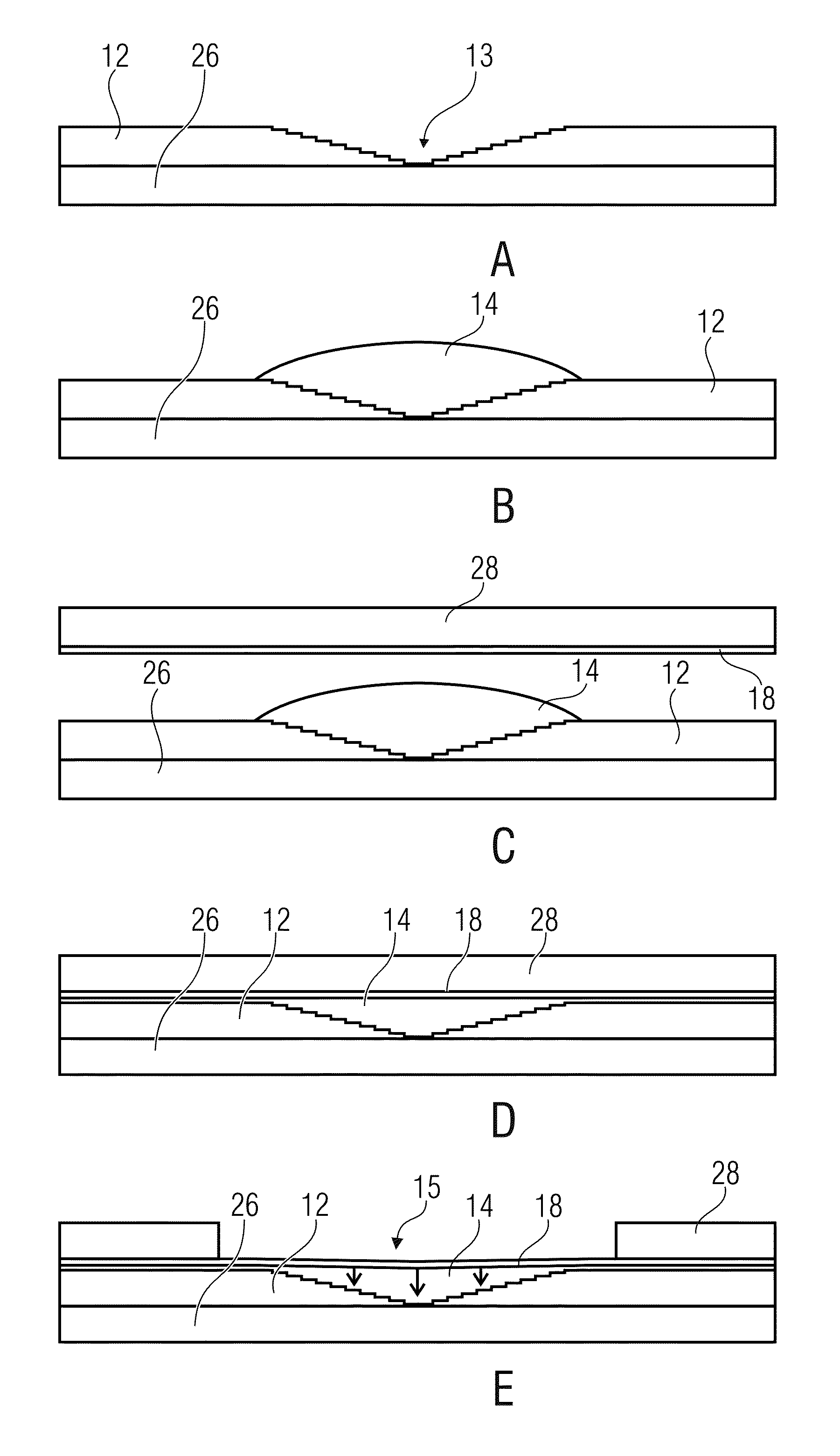
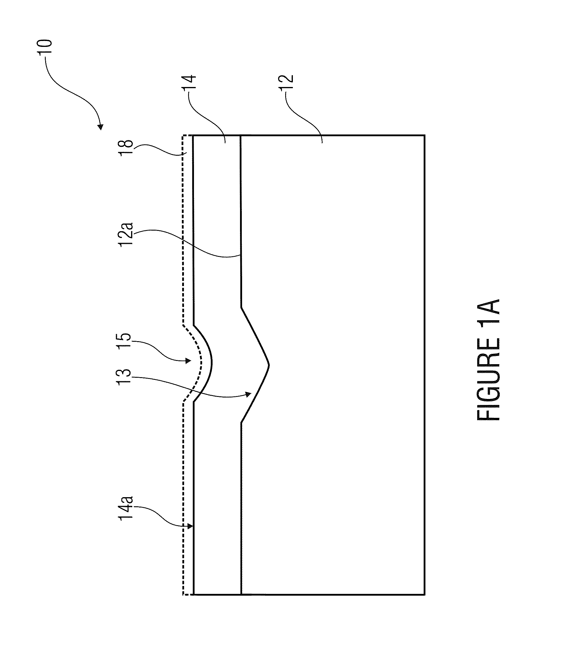
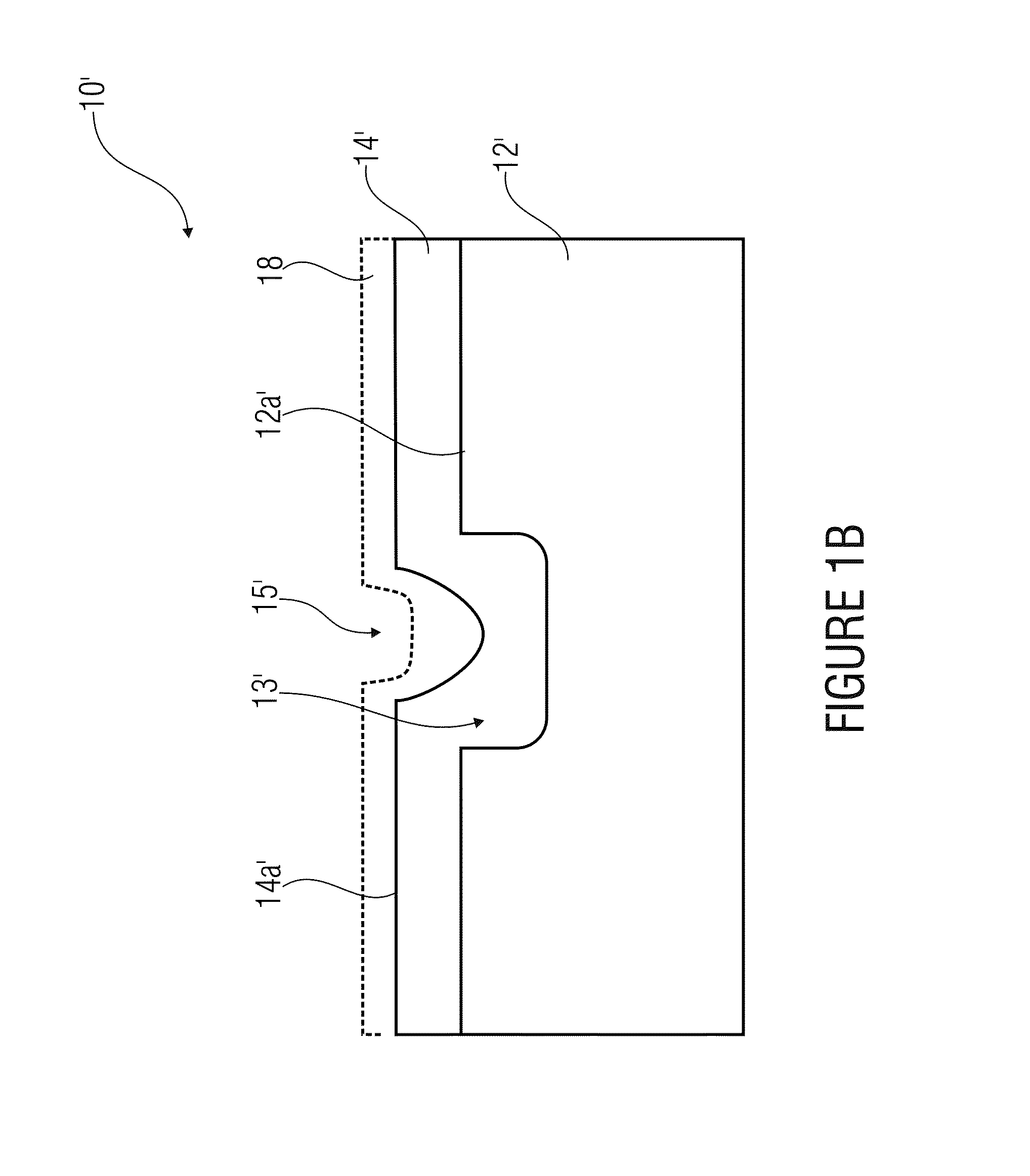
[0026]FIG. 1a shows an optical element 10 in the sectional representation with a structured carrier layer 12 and a layer 14 of cured material, which is arranged on the structured carrier layer 10, or on a first main surface 12a thereof. For example, the structured carrier layer 12 may be a photoresist applied to a substrate, or may be a structured substrate such as a glass or silicon substrate (silicon wafer), for example. The carrier layer 12 has, e.g., a thickness of 100 μm or generally a thickness within a range from 5 μm to 2 mm. The cured layer 14 typically includes a dielectric such as a polymer, PU (polyurethane) or a silicone (PDMS: polydimethylsiloxane), for...


PUM


Abstract

An optical element includes a structured carrier layer having a macrostructure at a main surface and a layer of cured material. The layer of cured material includes an optically smooth surface facing away from the main surface, a macrostructure surface of the surface being dependent on the macrostructure of the carrier layer and on a layer thickness profile of the layer.

Description

CROSS-REFERENCE TO RELATED APPLICATIONS[0001]This application claims priority from German Patent Application No. 102012219655.2, which was filed on Oct. 26, 2012, and is incorporated herein in its entirety by reference.[0002]Embodiments of the present invention relate to an optical element and to a method of producing same.BACKGROUND OF THE INVENTION[0003]Optical elements are understood to include gratings, lenses or curved mirrors, for example. Said optical elements typically comprise smooth surfaces with, e.g., curved, spherical, aspherical or parabolic surface functions. The optical properties are defined by the surface function, in particular via the radius of curvature.[0004]Optical elements are being increasingly miniaturized, which opens up the possibilities of combining different technologies, e.g. optics and electronics. Products originating from this field provide, e.g., electrically adaptable micro-optical systems wherein the optical properties may be adjusted externally,...

Claims


Application Information

Patent Timeline
IPC IPC(8): G02B5/18
CPCG02B5/1847G02B5/1861G02B5/18G02B3/00G02B5/10
Inventor WALLRABE, ULRIKEBRUNNE, JENSPAULS, MICHAELGRUNWALD, RUEDIGER
Owner ALBERT LUDWIGS UNIV FREIBURG
Why Eureka
Try Eureka