
Electrophotographic photoconductor, image forming apparatus, and process cartridge

Inactive Publication Date: 2014-05-01
RICOH KK
View PDF1 Cites 5 Cited by
  • Summary
  • Abstract
  • Description
  • Claims
  • Application Information

AI Technical Summary

Benefits of technology

The present invention provides an electrophotographic photoconductor with high wear resistance, durability, and excellent electrophotographic properties. This product can form stable images for a long time, solving the problems that previously existed.

Problems solved by technology

However, conventional organic photoconductors have a poor mechanical strength to have their photoconductive layer wear from a long time of use, and cannot perform proper image formation when the photoconductive layer has been worn out by a certain amount, because this entails changes in the electric characteristics of the photoconductor.
However, the current situations are, a highly-durable electrostatic latent image bearing member, which has a high wear resistance and excellent electrophotographic properties and can perform stable image formation for a long time, and its associated techniques have not been obtained yet, and their urgent supply is requested.
However, even this proposed technique cannot be said to fully meet the recent years' rising requests to the photoconductors, and it is requested to realize wear resistance, electrophotographic properties, and durability that allows stable image formation for a long time, all at higher levels.

Method used


Image

  • Electrophotographic photoconductor, image forming apparatus, and process cartridge
  • Electrophotographic photoconductor, image forming apparatus, and process cartridge
  • Electrophotographic photoconductor, image forming apparatus, and process cartridge

Examples


example 1

[0165]An alkyd resin (BECKOLITE M-6401-50, 50% by mass solid content, manufactured by DIC Corporation) (15 parts by mass), and a melamine resin (SUPERBECKAMINE G-821-60, 60% by mass solid content, manufactured by DIC Corporation) (10 parts by mass) were dissolved in methyl ethyl ketone (50 parts by mass).

[0166]Titanium oxide (CR-EL manufactured by Ishihara Sangyo Kaisha, Ltd.) (45 parts by mass) was added thereto, and the resultant was subjected to dispersion for 36 hours with a ball mill using alumina balls as media, to thereby obtain an intermediate layer coating liquid.

[0167]An aluminum drum having a diameter of 40 mm and a length of 346 mm was coated with the obtained liquid, dried for 20 minutes at 140° C., to thereby form an intermediate layer with a thickness of 3.0 μm.

[0168]Next, a butyral resin (S-LEC BMS manufactured by Sekisui Chemical Co., Ltd.) (5 parts by mass) was dissolved in cyclohexanone (20 parts by mass), an azo pigment having a structural formula (1) below (2 pa...

examples 2 , 3

Examples 2, 3, and 4, and Comparative Examples 1 and 2

[0176]An electrophotographic photoconductor was manufactured in the same manner as Example 1, except that the production of the protection layer coating liquid was changed as shown in Table 1 below. Table 1 also show d(1) / d(2), metal oxide content, and CXS3031P / AA-03.

TABLE 1d(1) / Metal oxideCXS303IP / CXS303IPAA-03d(2)contentAA-03Example 18.503.000.165.20.85Example 23.204.590.165.20.21Example 313.501.500.165.22.70Example 415.200.950.165.24.80Comparative18.500.000.165.2—Example 1Comparative0.005.550.165.20Example 2*Comparative Example 1 used only CXS303IP, and Comparative Example 2 used only AA-03

[0177]The electrophotographic photoconductors of Examples 1 to 4 and Comparative Examples 1 and 2 manufactured in the way described above were attached to the electrophotographic process cartridge of a digital full-color multi-functional machine (IMAGIO MP C3500 manufactured by Ricoh Company Ltd.). The contact pressure of the cleaning blade ...

example 5

[0184]An alkyd resin (BECKOLITE M-6401-50, 50% by mass solid content, manufactured by DIC Corporation) (18 parts by mass), and a melamine resin (SUPERBECKAMINE L-145-60, 60% by mass solid content, manufactured by DIC Corporation) (10 parts by mass) were dissolved in methyl ethyl ketone (80 parts by mass).

[0185]Titanium oxide (CR-EL manufactured by Ishihara Sangyo Kaisha, Ltd.) (55 parts by mass) and PT-401M (manufactured by Ishihara Sangyo Kaisha Ltd.) (20 parts by mass) were added thereto, and the resultant was subjected to dispersion for 36 hours with a ball mill using alumina balls as media, to thereby obtain an intermediate layer coating liquid.

[0186]An aluminum drum having a diameter of 40 mm and a length of 346 mm was coated with the obtained liquid, dried for 20 minutes at 130° C., to thereby form an intermediate layer with a thickness of 2.5 μm.

[0187]Next, an azo pigment having the structural formula (I) given above (24.0 parts by mass) and a τ-type metal-free phthalocyanine...


PUM

PropertyMeasurementUnit
Lengthaaaaaaaaaa
Percent by massaaaaaaaaaa
Thicknessaaaaaaaaaa

Abstract

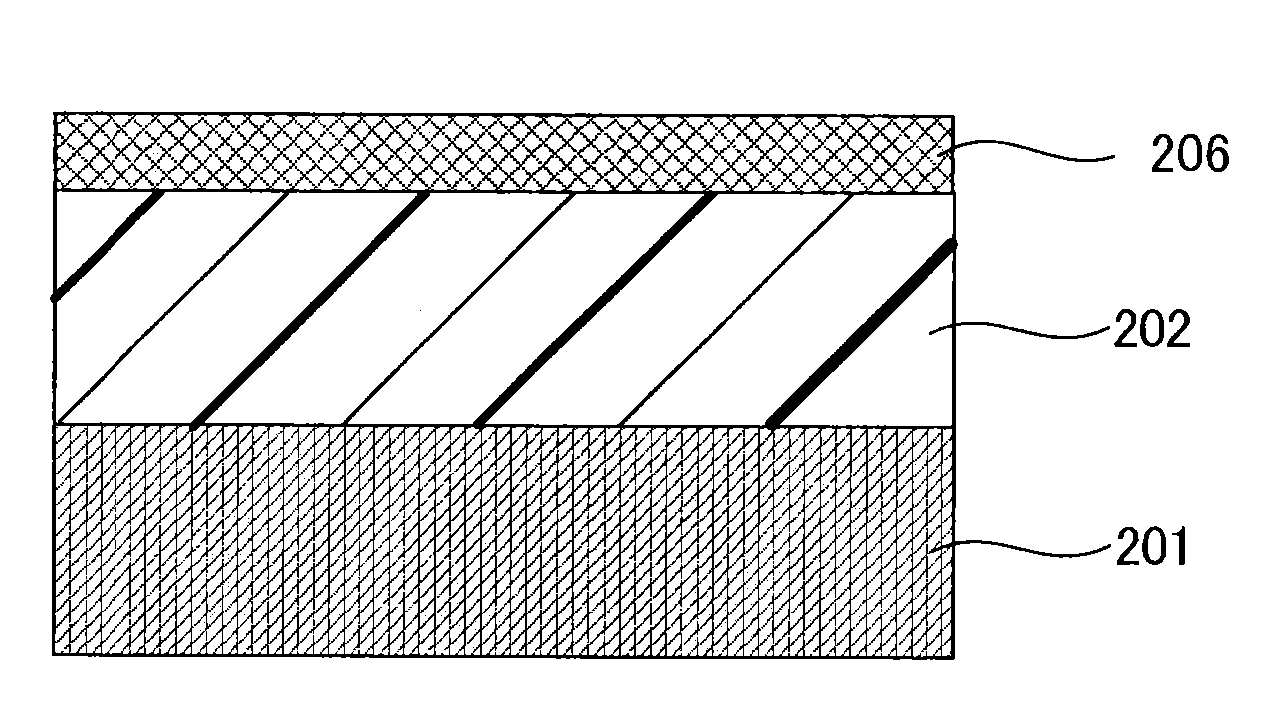
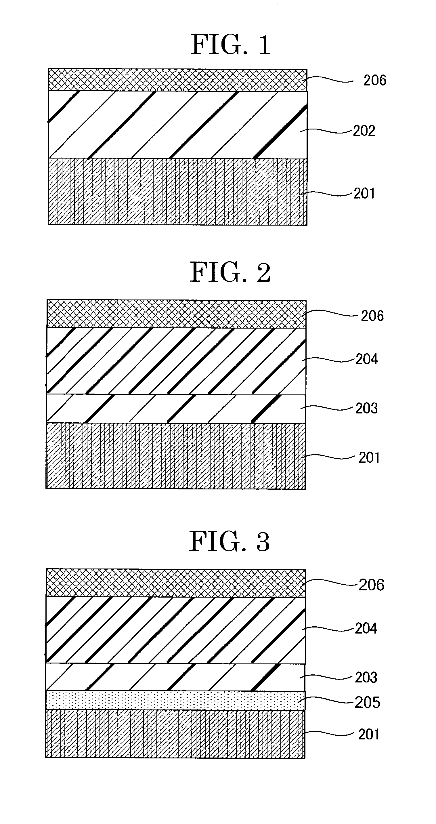
Provided is an electrophotographic photoconductor including an electroconductive substrate, a photoconductive layer on the electroconductive substrate, and a protection layer on the photoconductive layer, wherein the protection layer contains two or more metal oxides having different average primary particle diameters, a binder resin, and a charge transporting material, the content of the metal oxides in the protection layer is 50% by mass or higher, and the average primary particle diameters of the metal oxides satisfy all of formulae (I) to (III) below:d(1)<d(2)  formula (I);d(1) / d(2)≦0.25  formula (II); and0.1 μm≦d(2)  formula (III)where d(1) represents the average primary particle diameter (μm) of one metal oxide of the two or more metal oxides contained in the protection layer, and d(2) represents the average primary particle diameter (μm) of another or the other metal oxide of the two or more metal oxides contained in the protection layer.

Description

BACKGROUND OF THE INVENTION[0001]1. Field of the Invention[0002]The present invention relates to an electrophotographic photoconductor (hereinafter may be referred to as “photoconductor”), an image forming apparatus, and a process cartridge.[0003]2. Description of the Related Art[0004]Image forming apparatuses such as copiers, printers, and facsimile machines employing an electrophotographic system form an electrostatic latent image on a photoconductor by irradiating the photoconductor, which is uniformly charged, with writing light modulated with image data. Then, the image forming apparatuses form a toner image on the photoconductor on which the electrostatic latent image is formed, by supplying a toner to the photoconductor from a developing unit.[0005]Photoconductors that are most often used in such image forming apparatuses employing the electrophotographic system are organic photoconductors containing an organic photoconductive material. Organic photoconductors are advantageou...

Claims


Application Information

Patent Timeline
IPC IPC(8): G03G15/00G03G21/18
CPCG03G5/00G03G21/1814G03G2215/00957G03G5/0578G03G5/0507G03G5/0546G03G5/14704G03G5/14734G03G5/14773
Inventor YAMANAMI, HIROFUMIENOMOTO, KOJIESAKI, NAOYUKI
Owner RICOH KK
Learn More