
Ultrasonic measurement device, head unit, probe, and diagnostic device

a technology of ultrasonic measurement and diagnostic devices, which is applied in the direction of instruments, specific gravity measurement, applications, etc., can solve the problems of difficult downsizing of devices in which such an ic is installed, and achieve the effect of low voltage resistan

Inactive Publication Date: 2014-05-01
SEIKO EPSON CORP
View PDF13 Cites 15 Cited by
  • Summary
  • Abstract
  • Description
  • Claims
  • Application Information

AI Technical Summary

Benefits of technology

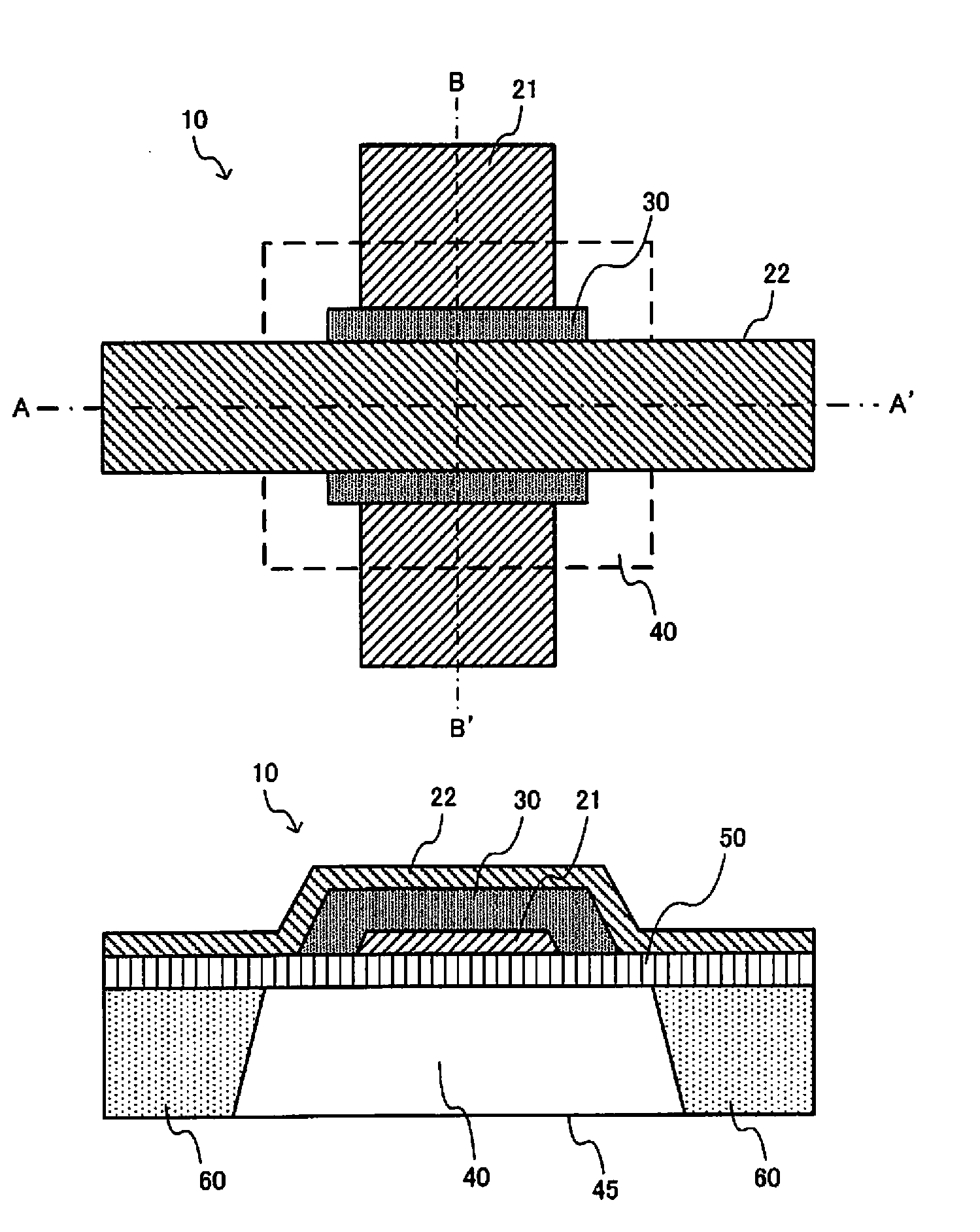
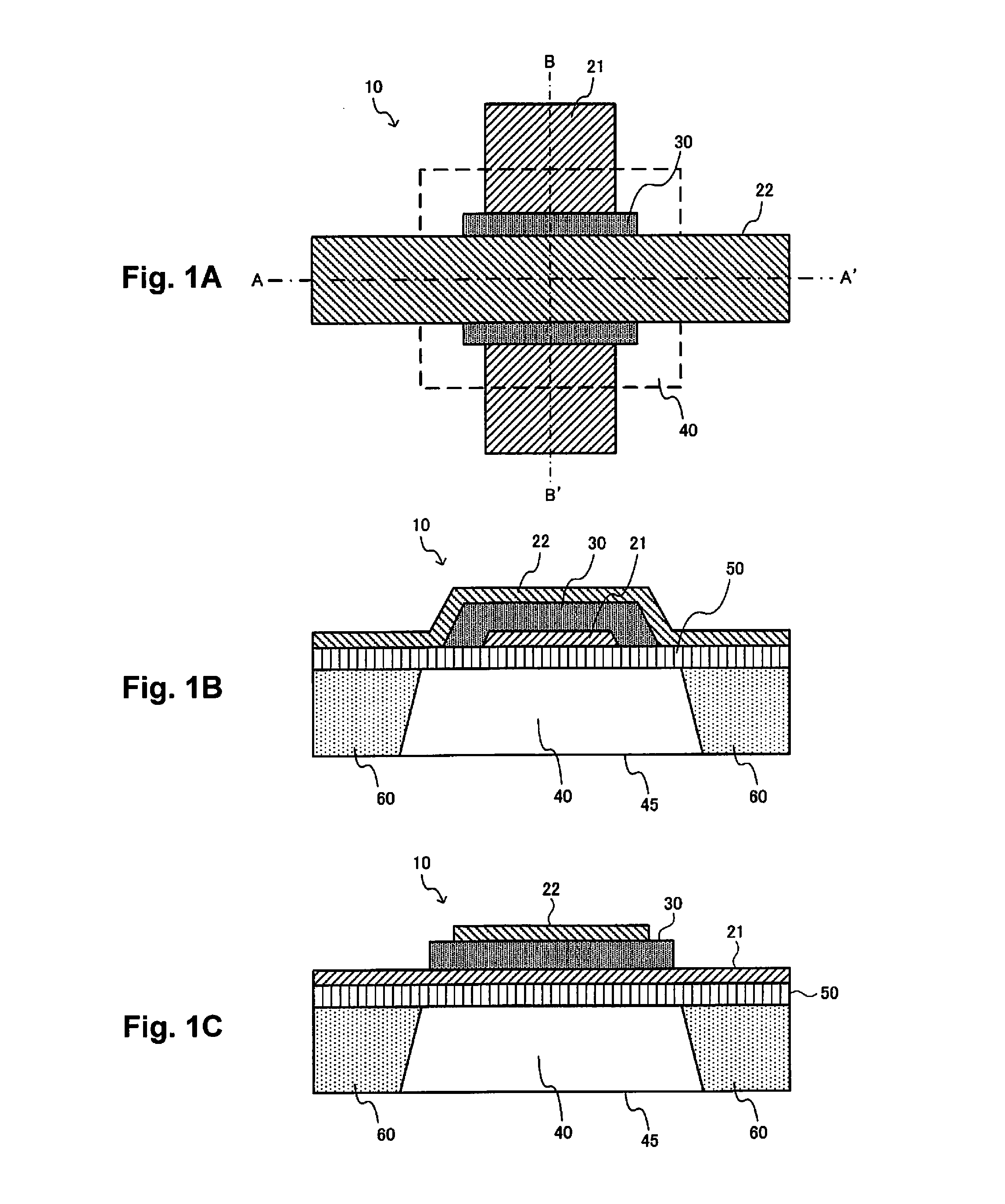
The present invention provides a way to make ultrasonic measurement devices, head units, and probes smaller in size. By using a piezoelectric element to vibrate a vibration film and create ultrasonic waves, the device can be driven with a low electric voltage and integrated circuit device can be manufactured in a compact way.

Problems solved by technology

Since an IC of high voltage resistance generally needs a large mounting area or the number of ICs becomes large, there is a problem that downsizing of a device in which such an IC is installed is difficult.

Method used


Image

  • Ultrasonic measurement device, head unit, probe, and diagnostic device
  • Ultrasonic measurement device, head unit, probe, and diagnostic device
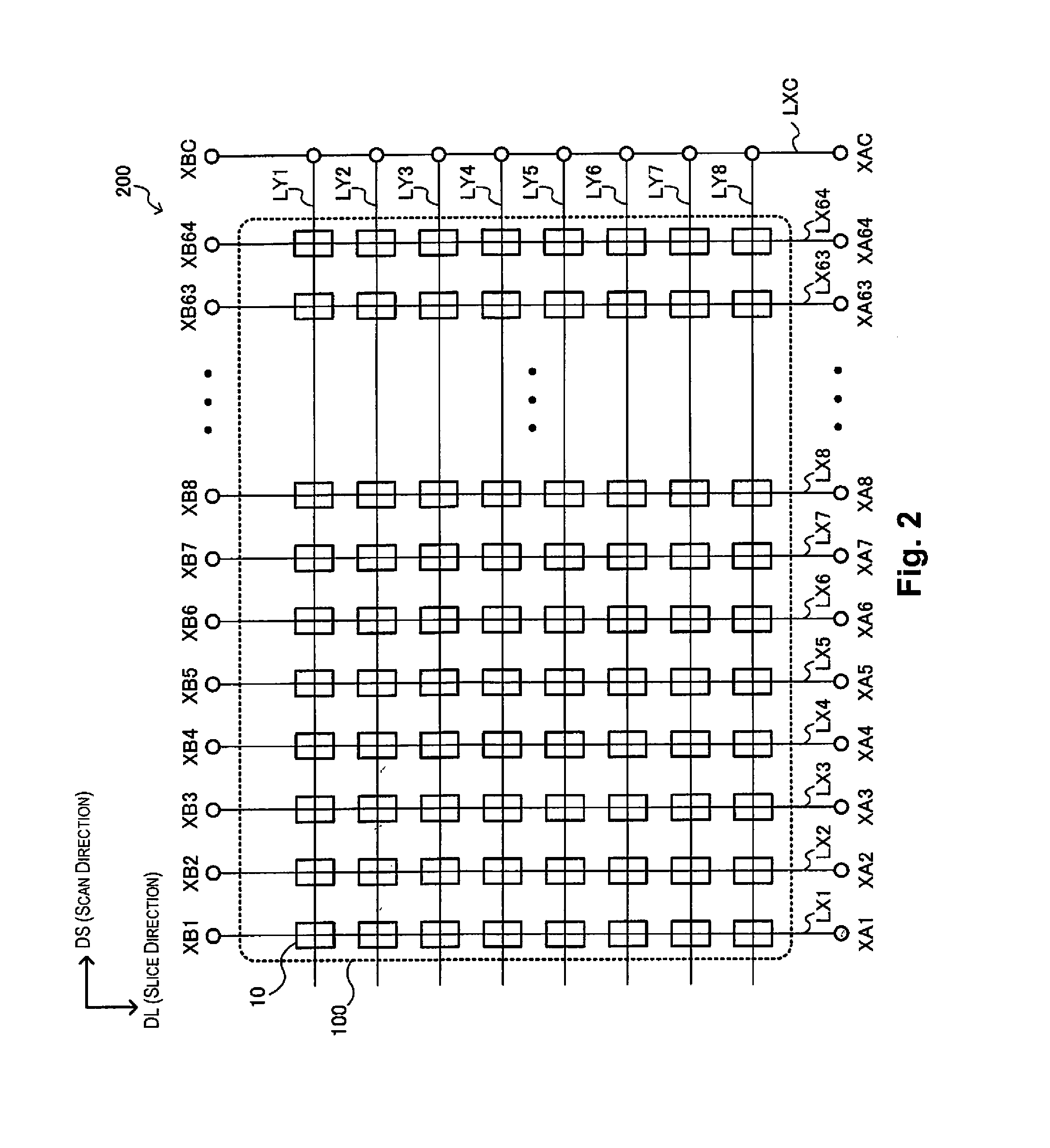
  • Ultrasonic measurement device, head unit, probe, and diagnostic device

Examples


Embodiment Construction

[0057]Next, preferred embodiments of the present invention will be explained in detail. The embodiments explained below shall not be construed as unreasonably limiting the subject matter of the present invention described in the claims, and all the elements explained in the embodiments are not necessarily essential to the solving means of the present invention.

1. Ultrasonic Element

[0058]As described above, when a bulk ultrasonic element, a driving IC of high voltage resistance is required, which causes a problem that downsizing of the device is difficult. For example, a portable ultrasonic measurement device or the like needs downsizing of the probe or the device itself. However, if a driving IC of high voltage resistance is installed, the downsizing will be hindered.

[0059]Further, in the above-described Japanese Laid-open Patent Publication No. 2005-341085, an electrode of a bulk piezoelectric member which is an ultrasonic element is connected to a transmission and reception sectio...


PUM


Abstract

An ultrasonic measurement device includes an ultrasonic transducer device, a flexible substrate, and an integrated circuit device. The ultrasonic transducer device has an ultrasonic element array, and a plurality of signal terminals. In the flexible substrate, a plurality of signal lines are formed along a first direction. The integrated circuit device is mounted on the flexible substrate such that a long side direction is along a second direction. The integrated circuit device has a plurality of terminals arranged along the second direction, and a transmission circuit provided for each of the terminals to output a transmission signal. Each of the terminals of the integrated circuit device is connected to a corresponding one of the signal lines of the flexible substrate. A plurality of the transmission circuits are arranged along the second direction in a state in which the integrated circuit device is mounted on the flexible substrate.

Description

CROSS-REFERENCE TO RELATED APPLICATIONS[0001]This application claims priority to Japanese Patent Application No. 2012-235419 filed on Oct. 25, 2012. The entire disclosure of Japanese Patent Application No. 2012-235419 is hereby incorporated herein by reference.BACKGROUND[0002]1. Technical Field[0003]The present invention relates to an ultrasonic measurement device, a head unit, a probe, a diagnostic device, and the like.[0004]2. Related Art[0005]In Japanese Laid-open Patent Publication No. 2005-341085, for example, an ultrasonic probe has been disclosed, in which an insulating material layer is provided from a part of a rear surface electrode of a bulk piezoelectric member to a side surface of the piezoelectric member, a conductive material layer is provided to be continuous with a front surface electrode of the piezoelectric member and wrap around to the rear surface electrode, and a wiring which is formed on a flexible substrate is connected to the conductive material layer and th...

Claims


Application Information

Patent Timeline
Patent Type & Authority Applications(United States)
IPC IPC(8): G01H11/08
CPCG01H11/08A61B8/4494A61B8/4411A61B8/4483
Inventor ENDO, KOGO
Owner SEIKO EPSON CORP
Learn More