Semiconductor device, method for manufacturing the semiconductor device, and method for controlling the semiconductor device
a semiconductor device and semiconductor technology, applied in the direction of pulse technique, power conversion system, electronic switching, etc., can solve the problems of increasing the total electric loss of the a-npc circuit, increasing the turn-on loss eon of the igbts b>101/b> and b>102/b> constituting the main switch b>100/b>, etc., to reduce the peak of reverse recovery current and suppress the peak
- Summary
- Abstract
- Description
- Claims
- Application Information
AI Technical Summary
Benefits of technology
Problems solved by technology
Method used
Image
Examples
embodiment 1
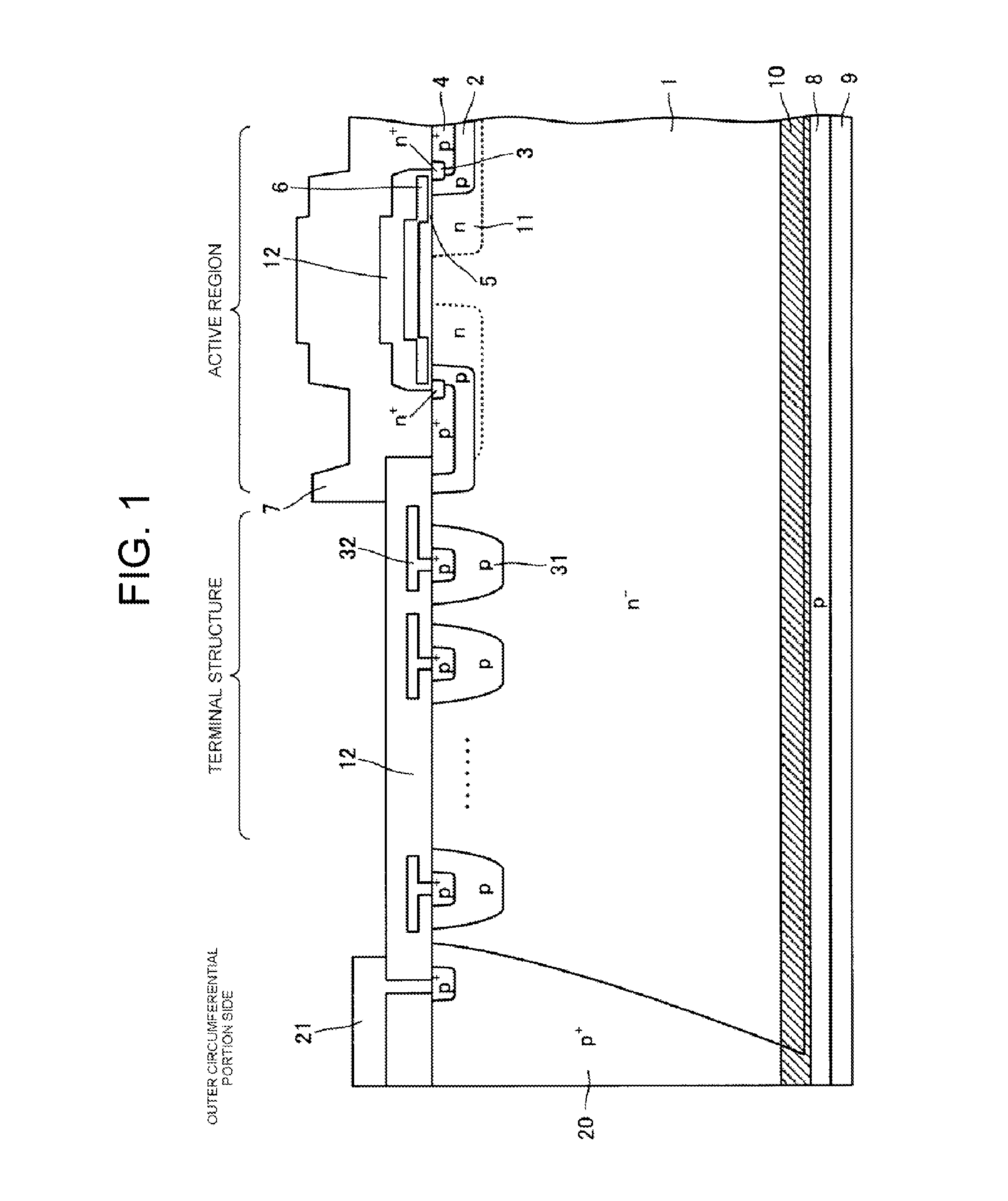
[0081]FIG. 1 is a sectional view showing the configuration of a semiconductor device according to Embodiment 1. The semiconductor device according to Embodiment 1 shown in FIG. 1 is an RB-IGBT which has a planar gate type MOS gate (insulated gate consisting of metal / oxide film / semiconductor) structure. As shown in FIG. 1, the semiconductor device according to Embodiment 1 has an active region and a terminal structure portion in an n− drift region (first semiconductor region) 1 consisting of an n− type semiconductor substrate (chip). A drift current flows into the active region which is surrounded by the terminal structure portion. The n− drift region 1 has a comparatively long carrier life time as compared with a typical device of an NPT structure. In the active region, a p base region (second semiconductor region) 2 is selectively provided in a surface layer of one side of the n− drift region 1.
[0082]An n region 11 is provided between the n− drift region 1 and the p base region 2. ...
embodiment 2
[0090]Next, the configuration of a semiconductor device according to Embodiment 2 will be described. FIG. 2 is a sectional view showing the configuration of a semiconductor device according to Embodiment 2. The semiconductor device according to Embodiment 2 is different from the semiconductor device according to Embodiment 1, in that grooves 22 are provided in the outer circumferential portion of the n− drift region 1, and the thickness of the n− drift region 1 is smaller on the outer circumferential portion side than on the active region side.
[0091]Specifically, as shown in FIG. 2, p+ isolation regions 20a are provided in the outer circumferential portion of the n− drift region 1 so as to extend from one side of the n− drift region 1 and at a smaller depth than the thickness of the n− drift region 1. In addition, grooves 22 are provided in the outer circumferential portion of the n− drift region 1 so as to extend from the other side of the n− drift region 1 and reach the p+ isolati...
embodiment 3
[0094]Next, a method for manufacturing a semiconductor device according to Embodiment 3 will be described in the case in which the semiconductor device according to Embodiment 2 is manufactured by way of example. FIGS. 3 to 5 are sectional views showing the state where the semiconductor device is being manufactured according to Embodiment 3. Here, a wafer is illustrated with the front surface up. However, the face of the wafer is reversed appropriately in each step (the same thing can be applied to FIGS. 6 to 19). First, as shown in FIG. 3, an n− type wafer serving as the n− drift region 1 (hereinafter referred to as “n− type wafer 1”) is prepared. Next, the p+ isolation regions 20a are selectively formed in the surface layer of the front surface of the n− type wafer 1 by ion injection of p type impurities and thermal diffusion treatment. The depth of each p+ isolation region 20a is set to be smaller than the final thickness of the n− type wafer 1.
[0095]Next, a front surface element...
PUM
 Abstract
Description
Claims
Application Information
 - R&D
- Intellectual Property
- Life Sciences
- Materials
- Tech Scout
- Unparalleled Data Quality
- Higher Quality Content
- 60% Fewer Hallucinations
Browse by: Latest US Patents, China's latest patents, Technical Efficacy Thesaurus, Application Domain, Technology Topic, Popular Technical Reports.
© 2025 PatSnap. All rights reserved.Legal|Privacy policy|Modern Slavery Act Transparency Statement|Sitemap|About US| Contact US: help@patsnap.com


