Compact regular reconfigurable fabrics

a fabric and fabric technology, applied in the direction of semiconductor devices, logic circuits using elementary logic circuit components, electrical apparatus, etc., can solve the problems of increasing number, hindering design closure, and traditional vlsi manufacturing process cannot achieve desired resolution, etc., to achieve maximum device density, yield, and reliability. the effect of reducing manufacturing complexity

Inactive Publication Date: 2014-03-20
BOARD OF RGT THE UNIV OF TEXAS SYST
View PDF5 Cites 2 Cited by
  • Summary
  • Abstract
  • Description
  • Claims
  • Application Information

AI Technical Summary

Benefits of technology

[0007]Described herein are reconfigurable fabrics for sublithographic silicon VLSI circuits. Sublithographic fabrics are typically based on a regular layout pattern which is as simple as possible for minimum manufacturing complexity and maximum device density, yield, and reliability. Embodiments herein relate to configurable fabric layouts that may be used for sublithographic reconfiguration.

Problems solved by technology

As VLSI technology scales into the nanometer domain, the minimum layout feature size becomes less than photolithography wavelength, traditional VLSI manufacturing process can no longer achieve desired resolution.
As technology scales, such auxiliary layout features become increasingly complex, leading to increased process variables or design uncertainties which hinder design closure.
This lengthened design cycle combined with skyrocketing mask costs have prevented an increasing number of VLSI designs from moving to the most advanced technologies.
However, they are based on complex layout patterns, which are not expected to achieve satisfiable yield as technology continues to scale down.

Method used


Image

  • Compact regular reconfigurable fabrics
  • Compact regular reconfigurable fabrics
  • Compact regular reconfigurable fabrics

Examples


Embodiment Construction

[0024]It is to be understood the present invention is not limited to particular devices or methods, which may, of course, vary. It is also to be understood that the terminology used herein is for the purpose of describing particular embodiments only, and is not intended to be limiting. As used in this specification and the appended claims, the singular forms “a”, “an”, and “the” include singular and plural referents unless the content clearly dictates otherwise. Furthermore, the word “may” is used throughout this application in a permissive sense (i.e., having the potential to, being able to), not in a mandatory sense (i.e., must). The term “include,” and derivations thereof, mean “including, but not limited to.” The term “coupled” means directly or indirectly connected.

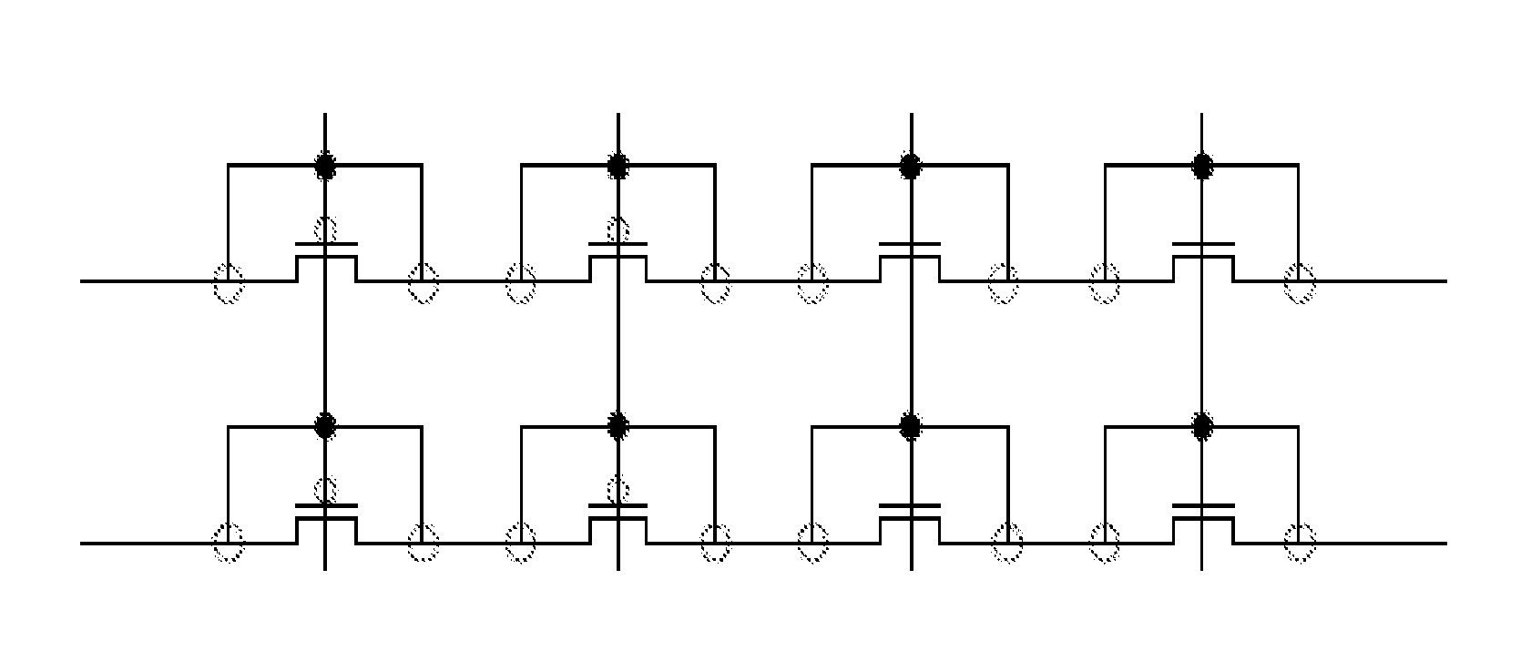
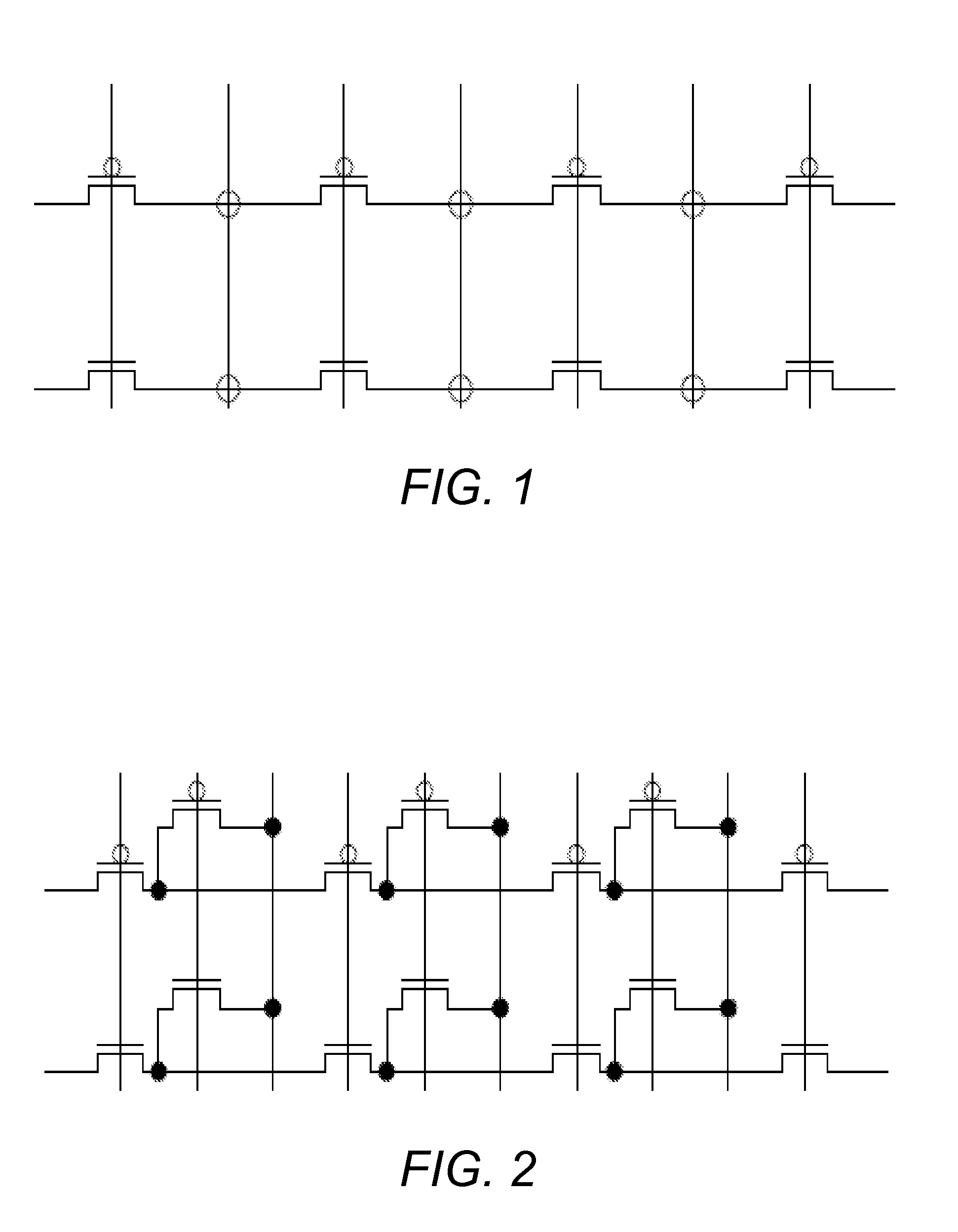
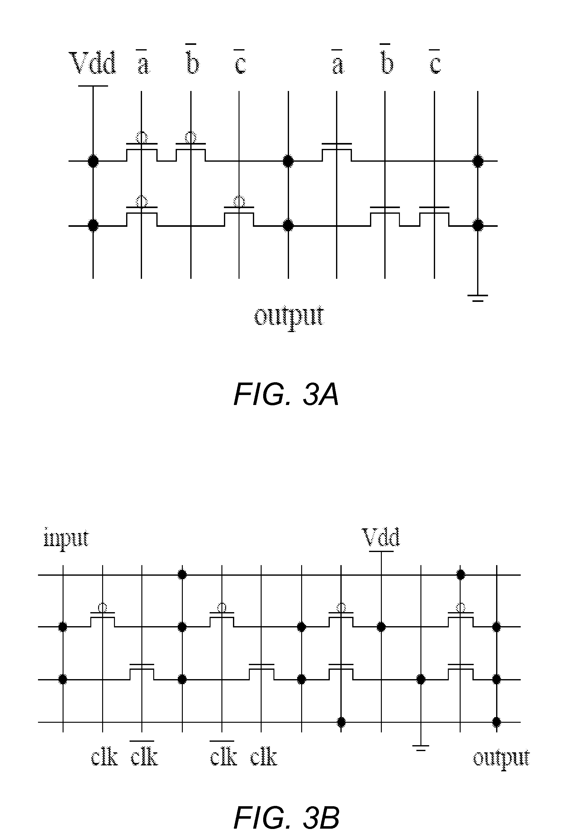
[0025]As VLSI technology continues to scale beyond the end of the roadmap for silicon based technologies, VLSI design is expected to be based on non-silicon nanoscale devices, e.g., carbon nanotubes (CNTs) and carbon...


PUM


Abstract

Described herein are compact regular programmable fabrics for improved logic density, yield, reliability, performance and power consumption compared with existing programmable fabric based VLSI design. Programmable fabrics facilitate technology transition from current silicon lithographic VLSI design to future non-silicon self-assembled nanoscale device based VLSI design.

Description

BACKGROUND OF THE INVENTION[0001]1. Field of the Invention[0002]The invention generally relates to configurable programmable semiconductor devices.[0003]2. Description of the Relevant Art[0004]As VLSI technology scales into the nanometer domain, the minimum layout feature size becomes less than photolithography wavelength, traditional VLSI manufacturing process can no longer achieve desired resolution. Optical Proximity Correction (“OPC”) and other Design for Manufacture (“DFM”) techniques enhance layout resolution by inserting auxiliary layout features. As technology scales, such auxiliary layout features become increasingly complex, leading to increased process variables or design uncertainties which hinder design closure. This lengthened design cycle combined with skyrocketing mask costs have prevented an increasing number of VLSI designs from moving to the most advanced technologies.[0005]Existing silicon based programmable Very Large Scale Integration (“VLSI”) fabrics include e...

Claims


Application Information

Patent Timeline
Patent Type & Authority Applications(United States)
IPC IPC(8): H01L27/118H01L27/02
CPCH01L27/0207H01L27/11807H03K19/177H10B41/40
Inventor LIU, BAO
Owner BOARD OF RGT THE UNIV OF TEXAS SYST
Why Eureka
Try Eureka