Sampling circuit, a/d converter, d/a converter, and codec

a sampling circuit and converter technology, applied in the field of sampling circuits and a/d converters, d/a converters, and codecs, can solve the problems of restricting the dispersion effect of conventional techniques, the inability to satisfactorily reduce the influence of generated noise on the other, and the inability to disperse periodic noise due to inrush current in an analog section, so as to reduce the influence of noise on electronic components, reduce the size of electronic components, and effectively suppress radiation nois

Active Publication Date: 2014-03-06
ASAHI KASEI ELECTRONICS CO LTD
View PDF4 Cites 3 Cited by
  • Summary
  • Abstract
  • Description
  • Claims
  • Application Information

AI Technical Summary

Benefits of technology

The present invention provides a sampling circuit that can reduce the impact of noise on electronic components in electronic devices. This is achieved by operating the sampling and holding section in response to a clock signal with added jitter. This advantage doesn't hinder the decrease in the size of electronic components or the process technology. Additionally, the continuous section can operate based on the clock signal with added jitter to effectively suppress radiation noise caused by inrush current.

Problems solved by technology

However, even when radiation noise generated from the D / A converter or the A / D converter is reduced as described in the conventional techniques, the influence of the generated noise on the other cannot be satisfactorily reduced.
In the conventional techniques, since the jitter is added to a digital section only, periodic noise due to inrush current in an analog section cannot be dispersed.
Accordingly, the dispersion effect of the conventional techniques is restrictive.
In this configuration, it is necessary to provide plural circuits for inputting the jitter, which hinders a decrease in the size of the electronic apparatus.

Method used


Image

  • Sampling circuit, a/d converter, d/a converter, and codec
  • Sampling circuit, a/d converter, d/a converter, and codec
  • Sampling circuit, a/d converter, d/a converter, and codec

Examples


embodiment 1

[0157]FIG. 15 is a diagram illustrating a pipelined A / D converter according to

[0158]The pipelined A / D converter according to Embodiment 1 is a converter that converts an analog input signal Ain into a digital output signal Dout of N bits. Accordingly, the pipeline type A / D converter includes a sampling circuit (which is described as S / H in the drawing) 801 that samples and holds the analog input signal Ain, k stages (which is described as S in the drawing) S1, S2, . . . , Sk that are connected in series to determine each bit, a memory 803 that stores an n-digit digital output signal dj (where j is an integer of 1 to k) determined in each stage, and a operational circuit 804 that calculates the digital output signal Dout which is the A / D converted value of the analog input signal Ain on the basis of the digital output signals dj stored in the memory 803.

[0159]In Embodiment 1, it is assumed that the A / D converter includes a control circuit 139 that controls plural stages. The control ...

embodiment 1-1

[0170 and Embodiment 1-2 will be described below as specific examples of the sampling circuit according to Embodiment 1. Embodiment 1-1 provides a sampling circuit using the clock signals φ1 and φ2 not having jitter added thereto and the clock signals φ1′ and φ2′ having jitter added thereto as clock signals. Embodiment 1-2 provides a sampling circuit using the clock signal φ1″ having jitter added to only the rising portion of the clock signal φ1 in addition to the clock signals φ1, φ2, φ1′, and φ2′. The basic configuration of the sampling circuit is the same in Embodiment 1-1 and Embodiment 1-2.

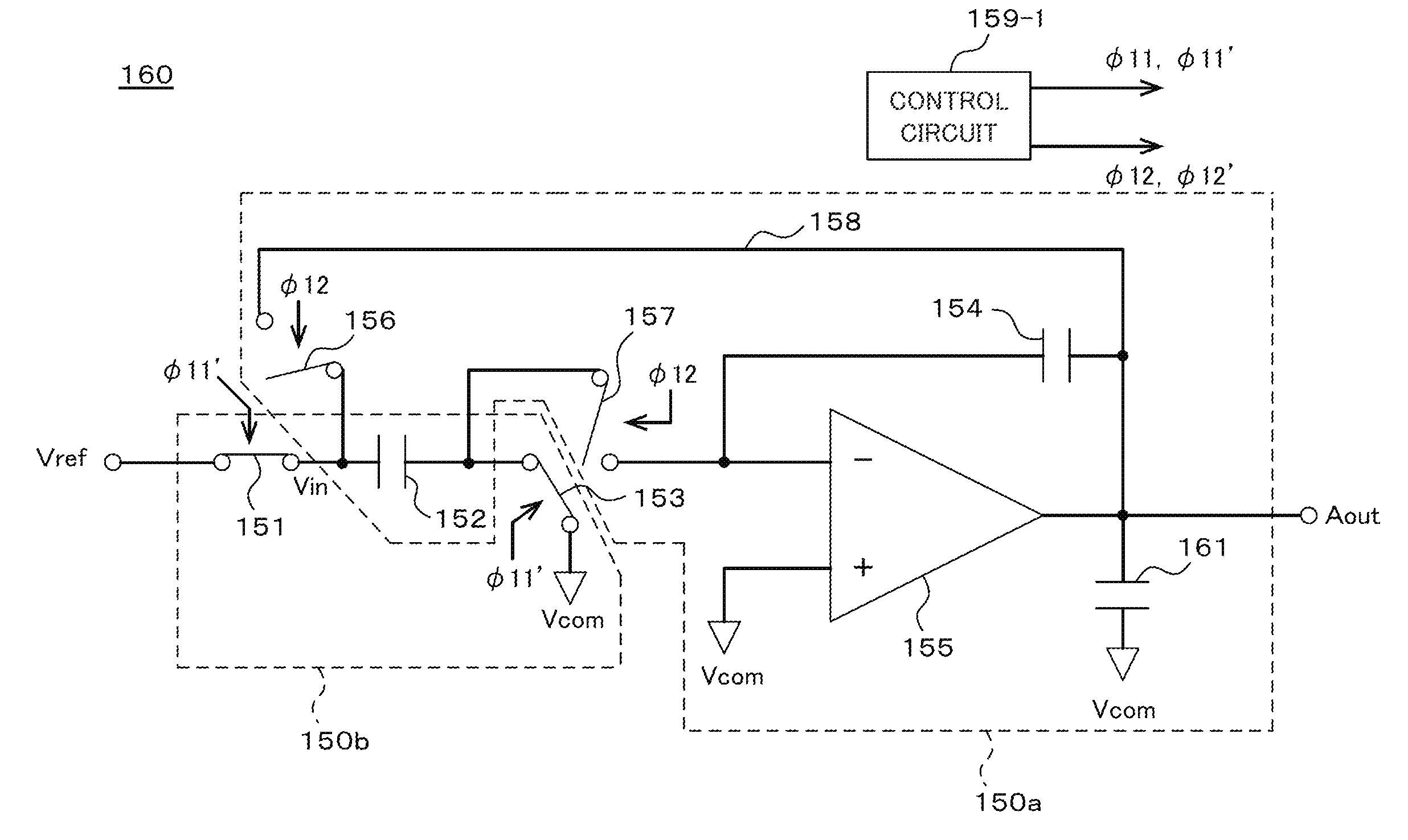
[0171]FIG. 17 is a diagram illustrating the sampling circuit according to Embodiment 1-1 and shows both the sampling circuit 801 shown in FIG. 15 and the control circuit 139 common to plural A / D converters.

[0172]The sampling circuit 140 (corresponding to the sampling circuit 801 shown in FIG. 15) shown in FIG. 17 includes a continuous section 130a that receives the analog input signal Ain and...

embodiment 2

[0217 will be described below.

[0218]In Embodiment 2, the sampling circuit according to the present invention is applied to a D / A converter.


PUM


Abstract

An A / D converter comprising: a sampling circuit including a continuous section, a sampling and holding section for intermittently sampling an input signal based on an analog signal input from the continuous section to hold and transfer the sampled signal, and a digital section for outputting a signal transferred from the sampling and holding section as a digital signal; and a control circuit for supplying a clock signal in which jitter is not added to the continuous section and supplying a clock signal in which the jitter is added to the sampling and holding section.

Description

TECHNICAL FIELD[0001]The present invention relates to a sampling circuit and an A / D converter, a D / A converter, and a CODEC, each including the sampling circuit.BACKGROUND ART[0002]At the present time, a decrease in the size of electronic devices are demanded more and more, the sizes of electronic components mounted on electronic devices are decreased, so that electronic components are arranged closer to each other. When such electronic components are arranged close to each other, noise generated in an electronic component may be transmitted to other electronic components directly or through a mounting board or wires and may hinder normal operations of other electronic components. Accordingly, suppression of an influence of noise along with a decrease in size are requested for electronic devices these years (hereinafter, referred to as anti-noise measures).[0003]In order to prevent noise generated in an electronic component from influencing on other electronic components, it is gene...

Claims


Application Information

Patent Timeline
IPC IPC(8): H03M1/12
CPCH03M1/1245H03M1/0656H03M1/12H03M1/66H03M1/1265
Inventor NAKANISHI, JUNYANAKANISHI, YUTAKANAKAMOTO, SEIKO
Owner ASAHI KASEI ELECTRONICS CO LTD
Why Eureka
Try Eureka